Logic Gates
A digital circuit with one or more input signals but only one output signal is called a logic gate. Since a logic gate is a switching circuit (i.e., a digital circuit), its output can have only one of two possible states: either a high voltage (1) or a low voltage (0) — it is either ON or OFF. Whether the output voltage of a logic gate is high (1) or low (0) depends on the conditions at its input.
The term logic is usually used to refer to a decision-making process. A logic gate makes logical decisions regarding the existence of the output depending upon the nature of the input. Hence, such circuits are called logic circuits.
A table that shows the conditions at the input and output of a logic gate in the binary form is called a truth table. The algebra used to symbolically describe logic functions is called Boolean algebra.
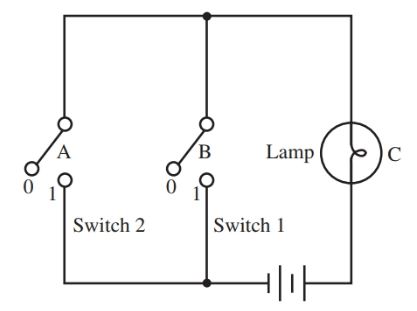
The basic idea of a logic gate using switches can be understood from Figure 1, where the output (OFF or ON) depends upon the conditions at the input.
- (i) When A and B are open, the lamp is OFF.
- (ii) When A is closed, and B is open, the lamp is ON.
- (iii) When A is open, and B is closed, the lamp is ON.
- (iv) When both A and B are closed, the lamp is ON.
This logic operation is known as OR operation and the logic is tabulated in Table 1 as follows:
| A | B | Lamp |
|---|---|---|
| Open | Open | OFF |
| Open | Closed | ON |
| Closed | Open | ON |
| Closed | Closed | ON |
Now, Table 1 can be written in the form of a Truth Table as follows:
| A | B | Y |
|---|---|---|
| 0 | 0 | 0 |
| 0 | 0 | 1 |
| 1 | 0 | 1 |
| 1 | 1 | 1 |
A logic gate is a circuit that has one or more input signals but only one output signal. All logic gates can be analysed by constructing a truth table. A truth table lists all input possibilities and the corresponding output for each input. The three basic logic gates that make up all digital circuits are (i) the OR gate, (ii) the AND gate, and (iii) the NOT gate. The following points may be noted about logic gates :
- (i) A binary 0 represents 0 V and binary 1 represents +5 V. It is common to refer to binary 0 as a LOW input or output and binary 1 as a HIGH input or output.
- (ii) A logic gate has only one output signal. The output will depend on the input signal(s) and the type of gate.
- (iii) The operation of a logic gate may be described either by truth table or Boolean algebra.
OR Gate
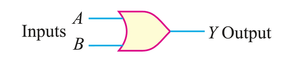
An OR gate is a logic gate that has two or more inputs but only one output. However, the output Y of an OR gate is LOW when all inputs are LOW. The output Y of an OR gate is HIGH if any or all the inputs are HIGH.
It is called OR gate because the output is high if any or all the inputs are high. For the same reason, an OR gate is sometimes called any or all gate. For example, consider a 2-input OR gate. The output Y will be high if either or both inputs are high.
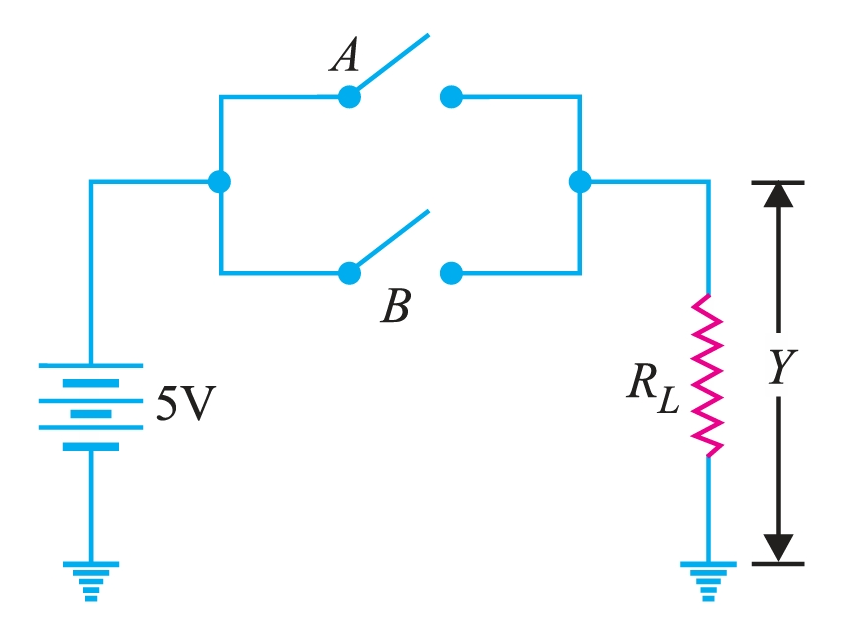
Figure 2 illustrates one method for constructing a 2-input OR gate. The input voltages are labeled as A and B while the output voltage is Y. Note that negative terminal of the battery is grounded and corresponds to 0 state (LOW level). The positive terminal of the battery (+5 V) corresponds to 1 state (HIGH level). There are only four input-output possibilities.
- (i) When both A and B are open, the resistance is non-conducting. Hence, the output voltage is zero. In terms of binary, when A = 0 and B = 0, then Y = 0.
- (ii) When A is OFF, and B is ON, the resistance \(R_{L}\) is conducting. In terms of binary, when A = 0 and B = 1, then Y = 1.
- (iii) When A is ON and B is OFF, the resistance \(R_{L}\) is conducting. In binary terms, when A = 1 and B = 0, then Y = 1.
- (iv) When both A and B are ON, then also the resistance \(R_{L}\) is conducting.
It is clear from the truth table that for the OR gate, the output is high if any or all of the inputs are high. The only way to achieve a low output is by having all inputs at a low level.
The + sign in Boolean algebra refers to the logical OR function. The Boolean expression for the OR function is
\[A + B = Y\]
The adjoining table shows the possible inputs. According to this table, when 0 is ORed with 0, the result equals 0. Also, any variable ORed with 1 equals 1. The OR function can be summed up as under :
0   ORed with 0 equals   0
0   ORed with 1 equals   1
1   ORed with 1 equals   1
The Boolean expression of the OR operation is given below:
| A + B = Y |
|---|
| 0 + 0 = 0 |
| 0 + 1 = 1 |
| 1 + 0 = 1 |
| 1 + 1 = 1 |
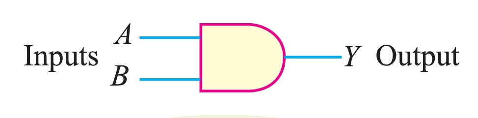
AND Gate
The AND gate is a logic gate that has two or more inputs but only one output. The output Y of the AND gate is HIGH when all inputs are HIGH. However, the output Y of the AND gate is LOW if any or all inputs are LOW.
It is called an AND gate because the output is HIGH only when all the inputs are HIGH. For this reason, the AND gate is sometimes called all or nothing gate. For example, consider a 2-input AND gate. The output will be HIGH when both the inputs are HIGH. AND gate operation. There are only four input-output possibilities.
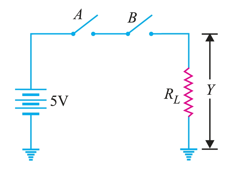
Figure 4 illustrates one method for constructing a 2-input AND gate.
- (i) When both A and B are OFF, then the resistor \(R_{L}\) is not conducting. In terms of binary, when A = 0 and B = 0, then Y = 0.
- (ii) When A is OFF, and B is ON, then the resistor is not conducting. Again output voltage will be zero. In binary terms, when A = 0 and B = 1, then Y = 0.
- (iii) When B is ON, and A is OFF, then also the resistor is not conducting. In binary terms, when A = 1 and B = 0, then Y = 0. (iv) When both A and B are ON, then the resistor is conducting. Now, the output voltage is +5 V through RL. It is clear from the truth table that for the AND gate, the output is high if all the inputs are high. However, the output is low if any or all inputs are low.
The Boolean expression for the AND function is
\[A . B = Y\]
where the multiplication dot stands for the AND operation. The adjoining table shows the possible inputs. The table tells us that 0 ANDed with any variable equals 0. Also, 1 ANDed with 1 equals one. The AND function can be summed up as under :
0 ANDed with 0 equals 0
0 ANDed with 1 equals 0
1 ANDed with 1 equals 1
The Boolean expression of the OR operation is given below:
| A . B = Y |
|---|
| 0 . 0 = 0 |
| 0 . 1 = 0 |
| 1 . 0 = 0 |
| 1 . 1 = 1 |
NOT Gate or Inverter
The NOT gate or inverter is the simplest of all logic gates. It has only one input and one output, where the output is the opposite of the input. The NOT gate is often called an inverter because it inverts the input.
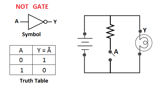
Figure 6 shows a typical inverter circuit.
- (i) When A is OFF, the current flows through the load resistor \(R_{L}\) to ground, and the output is + 5 V. In binary terms, when A = 0, Y = 1.
- (ii) When A is ON, then the current flows through A, and no current flows through the load resistor \(R_{L}\). Therefore, the output voltage is zero. In binary terms, when A = 1, Y = 0.
| A | Y=\(\overline{A}\) |
|---|---|
| 0 | 1 |
| 1 | 0 |
Table. 2 shows the truth table for an inverter.
It is clear from the truth table that, regardless of the input to the inverter, the output assumes the opposite polarity. If the input is 0, the output will be 1; if the input is 1, the output will be 0.
Figure 6 shows the logic symbol for the NOT gate or inverter. The small bubble on the inverter symbol represents inversion.
The Boolean expression for the NOT function is
\[Y=\overline{A}\]
where the line above the input A represents inversion.
If \(A = 0\), then \(Y = \overline{0}\) or \(Y = 1\). If \(A = 1\), then \(Y = \overline{1}\) or \(Y = 0\).