Combination of Basic Logic Gates
The OR, AND, and NOT gates are the three basic circuits that make up all digital circuits. In this topic, a few combinations of these basic circuits are discussed.
NAND gate
It is a combination of an AND gate and a NOT gate. In other words, the output of the AND gate is connected to the input of a NOT gate, as shown in Figure 1. Clearly, the output of a NAND gate is opposite to that of an AND gate. This is illustrated in the truth table for the NAND gate. The truth table for the NAND gate is developed by inverting the outputs of the AND gate.
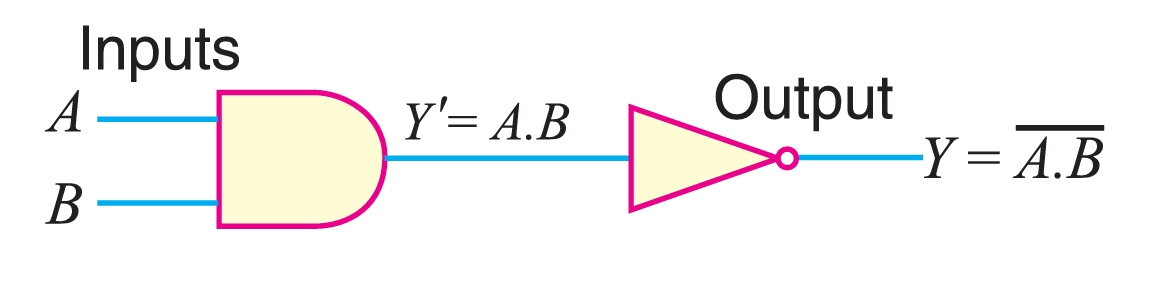
The Boolean expression for the NAND function is
\[Y = \overline{A · B}\]
This Boolean expression can be read as Y = not A . B. To perform the Boolean algebra operation, first the inputs must be ANDed, and then the inversion is performed. The output from a NAND gate is always 1 except when all of the inputs are 1.
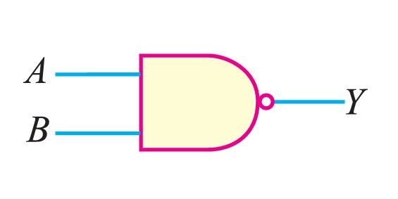
Figure 2 shows the logic symbols for a NAND gate. The little bubble (small circle) on the right end of the symbol means to invert the AND.
NOR gate
It is a combination of OR gate and NOT gate. In other words, the output of the OR gate is connected to the input of a NOT gate, as shown in Figure 3. The output of the OR gate is inverted to form a NOR gate. This is illustrated in the truth table for the NOR gate. It is clear that the truth table for the NOR gate is developed by inverting the outputs of the OR gate.
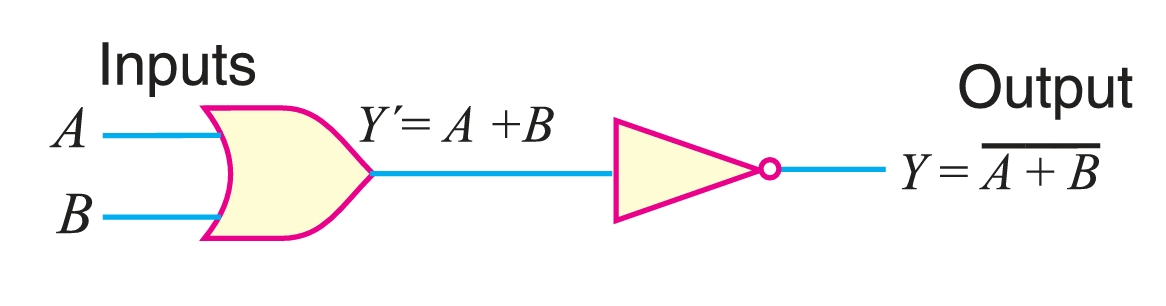
The Boolean expression for the NOR function is
\[Y = \overline{A + B}\]
This Boolean expression can be read as Y = not A or B. To perform the Boolean algebra operation, first the inputs must be ORed, and then the inversion is performed. Note that the output from a NOR gate is high (1) only when all the inputs are low (0). If any of the inputs is high (1), the output is low (0).
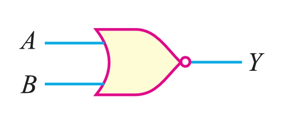
Figure 4 shows the logic symbol for a NOR gate. The small circle (bubble) at the Y output indicates inversion.
NAND Gate as a Universal Gate
The NAND gate is a universal gate because its repeated use can produce other logic gates. The table below shows how NAND gates can be connected to produce an inverter (i.e., NOT gate), an AND gate, and an OR gate.
- (i) NOT gate from NAND gate When two inputs of a NAND gate are joined together so that it has one input, the resulting circuit is a NOT gate. The truth table also shows this fact.
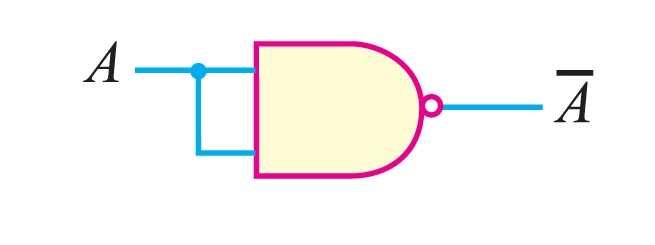
| \(A\) | \(B (= A)\) | \(Y\) |
|---|---|---|
| 0 | 0 | 1 |
| 1 | 1 | 0 |
- (ii) AND gate from NAND gates For this purpose, we use two NAND gates in a manner as shown above. The output of the first NAND gate is given to the second NAND gate, acting as an inverter (i.e., the inputs of the NAND gate are joined). The resulting circuit is the AND gate. The output Y′ of the first NAND gate (AND gate followed by NOT gate) is the inverted output of the AND gate. The second NAND gate acts as an inverter, further inverting it so that the final output Y is that of an AND gate.
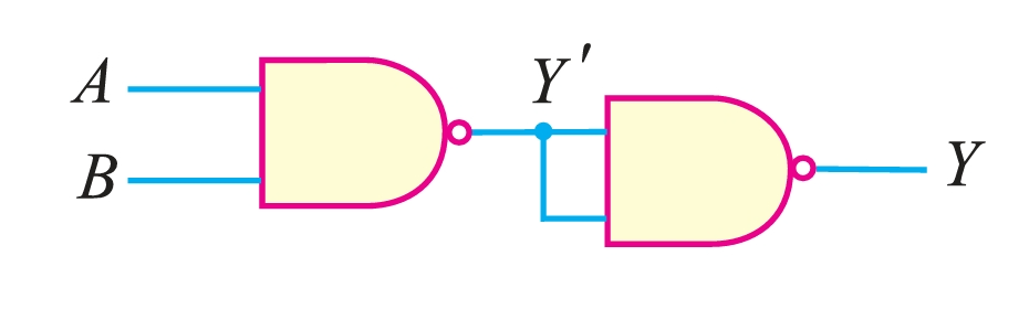
| \(A\) | \(B\) | \(Y^{′}\) | \(Y\) |
|---|---|---|---|
| 0 | 0 | 1 | 0 |
| 1 | 0 | 1 | 0 |
| 0 | 1 | 1 | 0 |
| 1 | 1 | 0 | 1 |
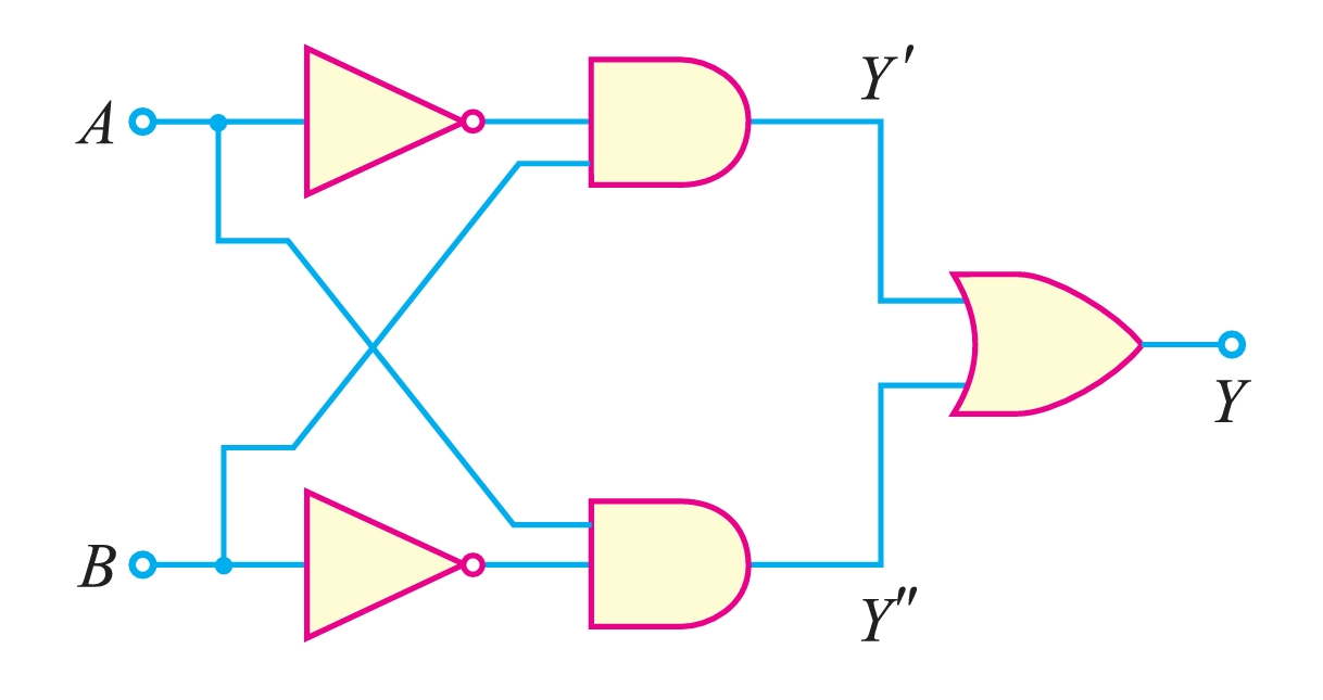
- (iii) OR gate from NAND gates For this purpose, we use three NAND gates in a manner as shown above. The first two NAND gates are operated as NOT gates, and their outputs are fed to the third. The resulting circuit is an OR gate.

| \(A\) | \(B\) | \(Y^{′} = A\) | \(Y^{″} = B\) | \(Y\) |
|---|---|---|---|---|
| 0 | 0 | 1 | 1 | 0 |
| 1 | 0 | 0 | 1 | 1 |
| 0 | 1 | 1 | 0 | 1 |
| 1 | 1 | 0 | 0 | 1 |
Exclusive OR Gate (XOR Gate)
The name exclusive OR gate is usually shortened to XOR gate. The XOR gate can be obtained by using OR, AND, and NOT gates, as shown in Figure 8.
The table shows the truth table for the XOR gate. The table shows that the output is HIGH (1) if any but not all of the inputs are HIGH (1). This exclusive feature eliminates the similarity to the OR gate. The OR gate truth table is also given so that you can compare the OR gate truth table with the XOR gate truth table.
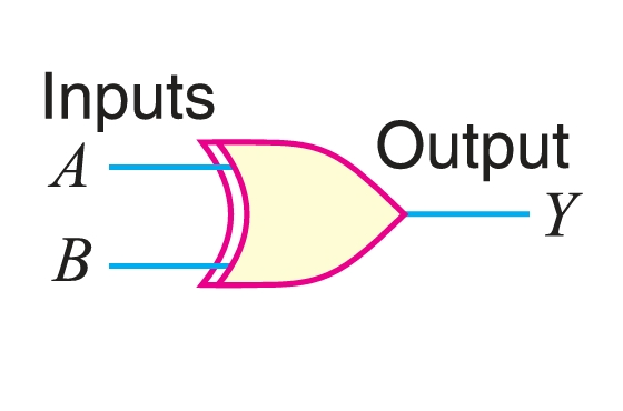
The logic symbol for the XOR gate is shown in Figure 9. The symbol is similar to that of an OR gate except for the additional curved line at the input side.
The logic operations in the circuit are as under :
| \(A\) | \(B\) | \(\overline{A}\) | \(\overline{B}\) | \(Y^{′} = \overline{A}·\overline{B}\) | \(Y^{′′}= \overline{A}·\overline{B} \) | \(Y = Y^{′} + Y^{′′}\) |
|---|---|---|---|---|---|---|
| 0 | 0 | 1 | 1 | 0 | 0 | 0 |
| 1 | 0 | 0 | 1 | 0 | 1 | 1 |
| 0 | 1 | 1 | 0 | 1 | 0 | 1 |
| 1 | 1 | 0 | 0 | 0 | 0 | 0 |