Combinational Logic Circuits
We can combine two or more logic gates to form a logic circuit or digital circuit. When the resulting logic or digital circuit has no feedback and no memory, it is often called a combinational logic circuit.
A logic circuit consisting of two or more logic gates that has no feedback and no memory is called a combinational logic circuit.
A combinational logic circuit is constructed using OR, AND, and NOT gates. Therefore, the basic building block for combinational circuits is the logic gate. Since a combinational logic circuit has no feedback and no memory, its output depends only on the current value of its inputs. A combinational logic circuit (or digital circuit) typically consists of multiple logic gates interconnected to perform a specific logic function. By using the laws, theorems, and techniques of Boolean algebra, we can find the Boolean expression for any combinational logic circuit.
Logic Circuit from its Boolean Expression
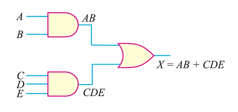
Consider the following Boolean expression :
\[X = AB + CDE\]
The function is composed of two terms, \(AB\) and \(CDE\), and it contains a total of five variables. The first term is formed by ANDing \(A\) and \(B\), and the second term is formed by ANDing \(C\), \(D\), and \(E\). These two terms are then ORed to form the function \(X\). The logic gates required to implement \(X = AB + CDE\) are as follows :
- (i) One two-input AND gate to form \(AB\).
- (ii) One three-input AND gate to form \(CDE\).
- (iii) One two-input OR gate to form the final function \(X (= AB + CDE)\).
The logic circuit that performs the function \(X = AB + CDE\) is shown in Figure 1.
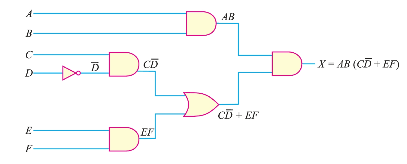
Consider the following Boolean expression :
\[X = AB (C\overline{D} + EF)\]
A breakdown of this equation shows that the term \(AB\) and the term \((C\overline{D} + EF)\) are ANDed. The term \(AB\) is formed by ANDing the variables \(A\) and \(B\). The term \(C\overline{D} + EF\) is formed first by ANDing \(C\) and \(\overline{D}\), ANDing \(E\) and \(F\), and then ORing these two terms. The logic gates required to implement \(X = AB (C\overline{D} + EF)\) are as follows :
- (i) One inverter to form \(\overline{D}\).
- (ii) Two two-input AND gates to form \(\overline{D}\) and \(EF\).
- (iii) One two-input OR gate to form \(\overline{D} + EF\).
- (iv) One two-input AND gate to form \(AB\).
- (v) One two-input AND gate to form \(X [= AB (C\overline{D} + EF)]\).
The logic circuit that forms the function \(X = AB (C\overline{D} + EF)\) is shown in Figure 2.
Truth Table from Logic Circuit
The output of a logic circuit for the given inputs can be determined directly from the circuit without using the Boolean expression. The procedure involves taking a given set of inputs and working through each gate of the circuit to determine the final output. Let us illustrate the procedure with an example. Consider the logic circuit shown in Figure 3. It consists of two AND gates and one OR gate. Each of the three gates has two input variables. Each of the input variables can be either a high (1) or a low (0). Since there are four input variables, there are 16 possible combinations of the input variables (24 = 16). We shall develop the truth table for the circuit without using the Boolean expression for the circuit.
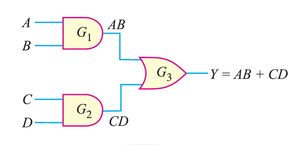
First, suppose each input is low (i.e., \(A = 0\), \(B = 0\), \(C = 0\), and \(D = 0\)). Under this condition, we shall examine the output of each gate in the circuit to arrive at the final output \(Y\). If the inputs to gate \(G1\) are low (0), the output of \(G1\) is low (0). Also, the output of \(G2\) is low (0) because both inputs are low (0). The two low inputs to \(G3\) also result in its output being low (0). Therefore, the output of the logic circuit is low when all the inputs are low, as shown in the truth table. Similarly, we can find the output of the circuit for the remaining 15 input combinations.
| Inputs | \(G1\) Output | \(G2\) Output | \(G3\) Output |
|---|---|---|---|
| \(ABCD\) | (\(AB\)) | (\(CD\)) | \(Y\) |
| 0 0 0 0 | 0 | 0 | 0 |
| 0 0 0 1 | 0 | 0 | 0 |
| 0 0 1 0 | 0 | 0 | 0 |
| 0 0 1 1 | 0 | 1 | 1 |
| 0 1 0 0 | 0 | 0 | 0 |
| 0 1 0 1 | 0 | 0 | 0 |
| 0 1 1 0 | 0 | 0 | 0 |
| 0 1 1 1 | 0 | 1 | 1 |
| 1 0 0 0 | 0 | 0 | 0 |
| 1 0 0 1 | 0 | 0 | 0 |
| 1 0 1 0 | 0 | 0 | 0 |
| 1 0 1 1 | 0 | 1 | 1 |
| 1 1 0 0 | 1 | 0 | 1 |
| 1 1 0 1 | 1 | 0 | 1 |
| 1 1 1 0 | 1 | 0 | 1 |
| 1 1 1 1 | 1 | 1 | 1 |
The logic circuit is shown in Figure 3. The Boolean expression for this logic circuit is
\[Y = AB + CD\]
Now simply put in the values for each combination of inputs and use the Boolean rules and laws to determine the final output \(Y\). For example, when \(A = 1\), \(B = 1\), \(C = 1\) and \(D = 0\), the final output is
| Y | = | \[AB + CD\] |
| = | 1.1 + 1.0 | |
| = | 1 + 0 | |
| = | 1 |
Similarly, we can find \(Y\) for the remaining 15 input combinations to get the truth table shown above. Also, we can construct the truth table by developing the Boolean expression from the logic circuit.