Extrinsic semiconductor
At 300 K the intrinsic carrier concentration is not very high in silicon and the numbers of electrons and holes are equal. Silicon is a covalently-bonded element with the same structure as diamond and germanium. Each silicon atom has four outer, bonding electrons and with them it forms four covalent bonds by which it is joined to four other silicon atoms arranged at the comers of a regular tetrahedron as in figure.
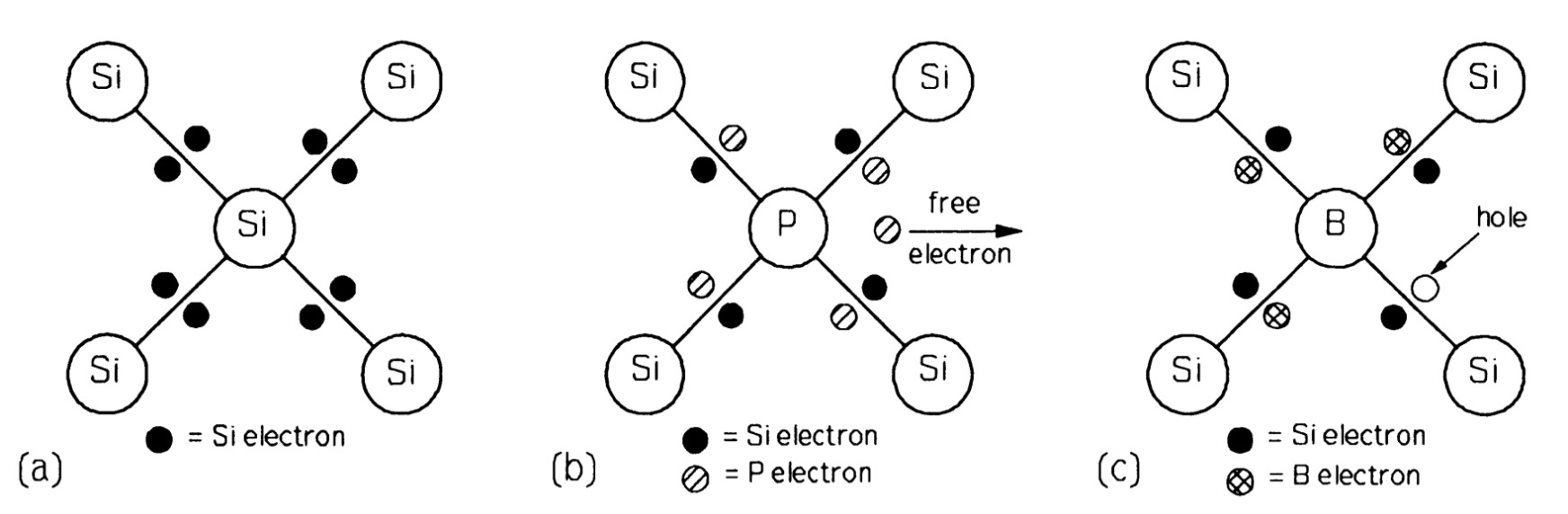
If an atom of silicon is replaced by one of phosphorus, which has five electrons available for bonding, then it can form four bonds with neighbouring silicon atoms, using up four electrons and having one left over. This spare electron is readily detached from its parent atom (the ionisation energy is of the order of \(10 m~eV\)) to move into the nearby conduction band; at \(300 K\) practically all the phosphorus atoms are ionised. The concentration of phosphorus atoms, \(N_{D}= n\), the conduction-electron concentration. Phosphorus is known as a donor atom because it donates electrons to the conduction band. Arsenic and antimony behave as donors in silicon too.
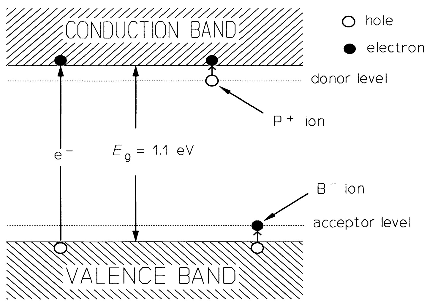
When an atom of boron is substituted for one of silicon the position is different, as boron has only three electrons available for bonding, as a result, when it forms four bonds with a neighbouring silicon atom as in figure, there is a deficiency of an electron -a hole - in one of the bonds. This hole can also move about freely in the valence band and acts as a mobile positive charge carrier, though really the electrons move the other way. The boron atoms are also effectively \(100 \%\) ionised in silicon (though negatively, not positively like phosphorus), so the concentration of boron atoms, \(N_{A}= p\), the hole concentration. Boron is termed an acceptor because it accepts an electron from a silicon atom. In semiconductor devices, the dopant atom concentration far exceeds the intrinsic carrier density; conduction is thus said to be extrinsic. Figure shows the energy levels in extrinsic silicon. The higher up an electron is in figure , the higher is its energy. However, for holes, the lower it is, the higher is its energy.
The law of mass action applies to the charge carrier concentration in a semiconductor, that is the product of electron and hole concentration, \(p-n\), is constant at constant temperature. If electrons predominate, the material is said to be \(n\)-type and the electrons are the majority carriers, holes the minority carriers. If holes predominate, the material is \(p\)-type, holes are the majority and electrons the minority carriers.