The p-n junction
Whether a particular piece of semiconductor is \(p\)-type, \(n\)-type or intrinsic makes no difference to the direction of (conventional) current flow when a voltage is applied to its ends, though the current's magnitude will depend on the doping level. But when \(p\)- and \(n\)-type materials are joined, or a \(p-n\) junction is formed, matters undergo a great transform-ation: current is now found to flow much more easily in one direction than in the other. The junction is a rectifier, or diode. \(p-n\) junctions, singly or in combinations of two or more, are essential for the operation of many semiconductor devices.
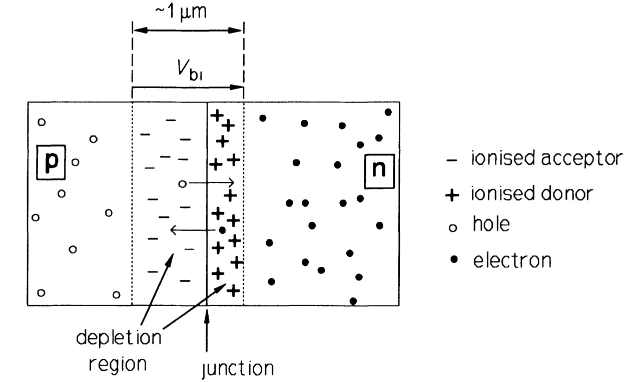
Figure 1 shows a cross-section of a \(p-n\) junction, with no externally applied potential.
Before the junction is formed the \(n\)-type material consists of fixed, positively-charged donor ions and an equal number of conduction electrons, while the \(p\)-type material consists of fixed, negatively-charged acceptor ions and an equal number of holes. When the junction is formed, electrons from the \(n\)-type region diffuse into the \(p\)-type region (leaving a fixed positive charge behind) and combine with holes. Simultaneously, holes from the \(p\)-type region diffuse into the \(n\)-type region (leaving a fixed negative charge behind) and combine with free electrons, thus causing an absence of mobile charge carriers in the junction region. In the depletion region (or zone) in the vicinity of the junction a voltage called the built-in potential, \(V_{bi}\) is thus set up which opposes the diffusion of charge carriers across the junction. \(V_{bi}\) is about \(0.6~V\) in silicon, about \(1.2 ~V\) in \(GaAs\) and about \(0.3 ~V\) in germanium. Thus with no bias applied, the diffusion current for the electrons (from then-region), \(I_{er}\) is exactly equal to the current (due to thermally generated electrons in the \(p\)-region), \(I_{eg}\) produced by \(V_{bi}\)· The same is true for the hole currents, \(I_{hg}\) and \(I_{hr}\). The holes and electrons move in opposite directions, though the conventional currents are in the same direction because of the negative electronic charge:
Thus
\[I_{ g} = I_{eg} + I_{hg}\].
When reverse bias is applied to the junction, that is the \(p\)-type side is made more negative than the \(n\)-type, the depletion region becomes larger as the bias voltage adds to \(V_{bi}\). The diffusion current, \(I_{r}\) that flows across the junction is very small, since only carriers with enough energy can surmount the potential barrier. But the current, \(I_{g}\), due to thermally generated minority carriers, remains unaffected by the bias field, resulting in a net reverse current, \(I_{g} - I_{r}\). When the junction is fotward biased (\(p\)-type side positive with respect to the \(n\)-type) the depletion zone is narrower than under zero bias and \(I_{r}\) is now very much greater than \(I_{g}\). Figure shows the effect of bias polarity on the depletion zone widths and the forward current.
Reverse current is often called leakage current and its magnitude depends on the material and the size of the diode. Germanium diodes have high leakage currents - about \(1,000\) times that of silicon diodes (a silicon signal diode at room temperature typically has a leakage of around \(1 nA\)). Light causes the generation of additional electron-hole pairs in semiconductors thereby increasing the leakage current. The so-called dark current is the leakage current when no light falls on the semiconductor material.
A glossary of terms
| Terms | Details |
|---|---|
| Acceptor | A dopant atom that has fewer valence electrons than the host semiconductor material, so that it can accept one or more electrons from the valence band of the host and gives rise to a corresponding number of holes in the valence band. Boron is an acceptor atom in silicon |
| Band gap | The energy difference, \(E_{g}\), between the top of the valence band and the bottom of the conduction band, usually given in electron volts (\(~eV\)), where \(1 ~eV = 1.6 \times 10^{-19} J\). In silicon the band gap is about \(1.1 ~eV\). |
| Bias | The potential applied to a \(p-n\) junction. Positive bias means that the \(p\)-type side of the junction is at a higher potential than the \(n\)-type side, negative bias means vice versa |
| Charge carrier compensation | Either a negatively-charged electron or a positively charged hole The reduction in charge-carrier concentration in a semiconductor that is brought about by incorporating both donors and acceptors into the semiconductor material. Hence reduced conductivity |
| Conduction band | A region of energy states lying above the valence band and separated from it by an energy gap in which electrons are not bound to their parent atoms and can move under the influence of applied fields |
| Conductivity | Defined by \(\sigma= nq\mu\), where \(n\) = charge carriers/\(m^{3}\), \(q\), the electronic charge = \(1.6 \times 10^{-19} C\), \(\mu\) = mobility (\(q.v.\)) in \(m^{2}/V/s\). The reciprocal of the resistivity (\(q.v.\)) |
| Conductivity type | Determined by the majority charge carriers. When these are electrons the material is \(n\)-type and when these are holes it is \(p\)-type |
| Depletion region | A volume of material near a \(p-n\) junction in which oppositely charged carriers have combined so that the mobile charge carrier concentration is very small |
| Donor | A dopant atom which has more valence electrons than its host semiconductor, so that it tends to give up electrons to the conduction band, so making the material \(n\)-type. Examples are phosphorus and arsenic in silicon |
| Dopant | An element which is incorporated in controlled amounts into a semiconductor during crystal growth. At working temperatures the dopant is ionised and supplies electrons or holes to the host to produce a vast excess of one or the other, so making the material \(p\)-type or \(n\)-type |
| Extrinsic conduction | Conduction brought about by charge carriers from ionised dopants |
| Hole | The absence of an electron in the valence band, which acts like a positively charged electron |
| Intrinsic conduction | Conduction by hole-electron pairs produced by ionisation of the semiconductor material. Ionisation means that electrons in the valence band must cross the band gap to reach the conduction band. At normal temperatures there are few carriers produced like this and conductivity is low |
| Majority carrier | The more-numerous charge-carrier. Electrons in \(n\)-type material, holes in \(p\)-type |
| Minority carrier | The less-numerous charge-carrier. Holes in \(n\)-type material, electrons in \(p\)-type |
| Mobility | The speed acquired by a charge carrier in unit electric field, \(\mu = v/E= \sigma/nq\) |
| p-n junction | The plane dividing \(p\)-type from \(n\)-type material, which lies within the depletion region resistivity valence band |
| Resistivity | Given by \(\rho = RA/l\), where \(R\) = resistance in \(\Omega\) measured between the ends of a bar of material, cross-sectional area \(A m^{2}\) and length \(l~m\) |
| Valance band | The region of energy states lying below the conduction band by \(E_{g}\), the gap energy. Holes are free to move in the valence band like electrons in the conduction band |