Biasing schemes of pn junction
The semiconductor diode, with applications too numerous to mention, is created by simply joining an \(n\)-type and a \(p\)-type material together, nothing more, just the joining of one material with a majority carrier of electrons to one with a majority carrier of holes.
No Applied Bias
\(V = 0 V\)
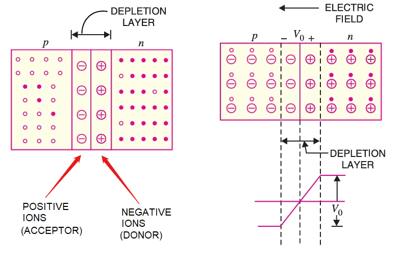
When the two materials are joined the electrons and the holes in the region of the junction will combine, resulting in a lack of free carriers in the region near the junction.
The only particles displayed in this region are the positive and the negative ions remaining once the free carriers have been absorbed.
*This region of uncovered positive and negative ions is called the depletion region due to the “depletion” of free carriers in the region. *
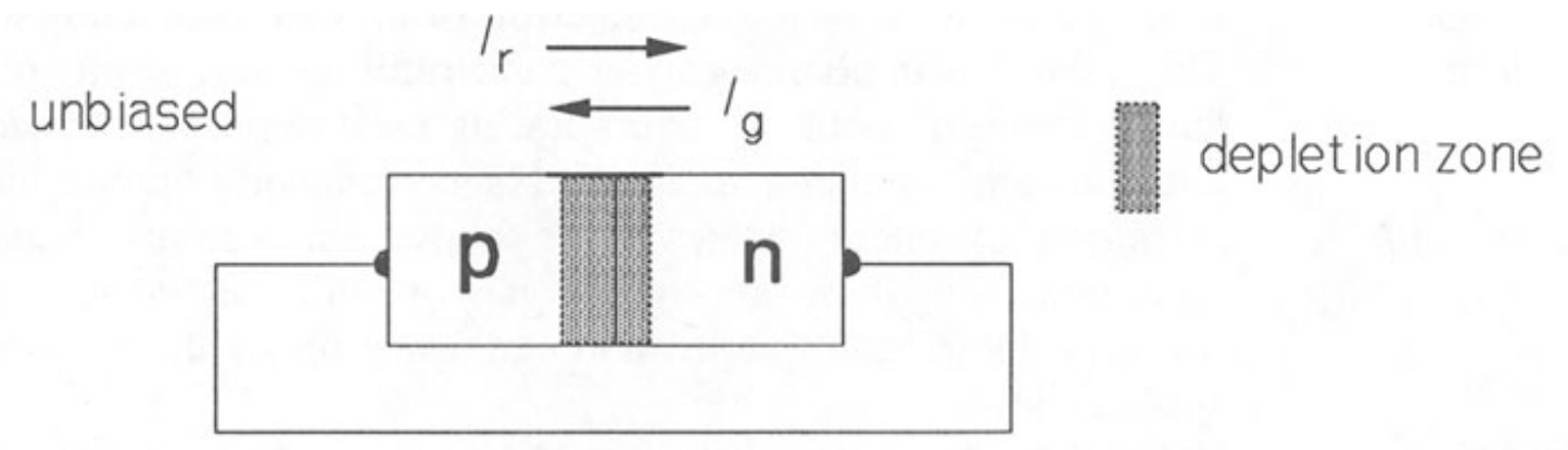
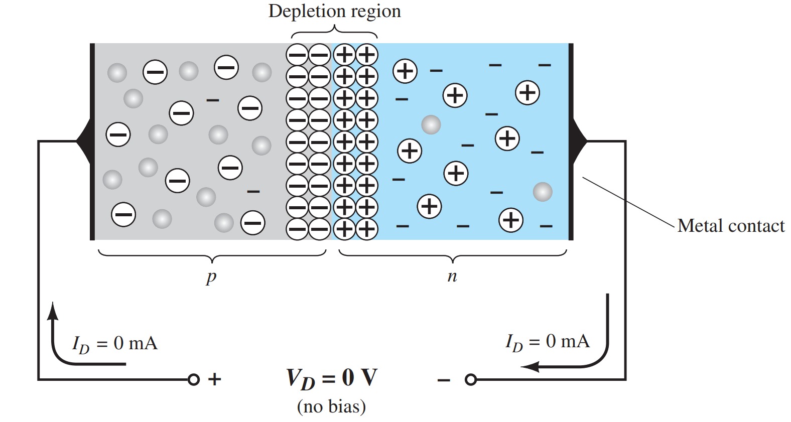
If leads are connected to the ends of each material, a two-terminal device results. Three options then become available: no bias, forward bias, and reverse bias. The term bias refers to applying an external voltage across the two terminals of the device to extract a response. The condition is the no-bias situation if no external voltage is applied.
The absence of a voltage across a resistor results in zero current through it.
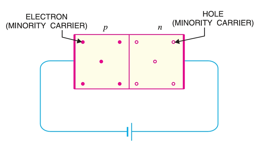
Under no-bias conditions, any minority carriers (holes) in the \(n\)-type material that find themselves within the depletion region for any reason whatsoever will pass quickly into the \(p\)-type material. The closer the minority carrier is to the junction, the greater the attraction for the layer of negative ions and the less the opposition offered by the positive ions in the depletion region of the \(n\)-type material. The majority of carriers (electrons) of the \(n\)-type material must overcome the attractive forces of the layer of positive ions in the \(n\)-type material and the shield of negative ions in the \(p\)-type material to migrate into the area beyond the depletion region of the \(p\)-type material. However, the number of majority carriers is so large in the \(n\)-type material that there will invariably be a small number of majority carriers with sufficient kinetic energy to pass through the depletion region into the \(p\)-type material. Again, the same type of discussion can be applied to the majority carriers (holes) of the \(p\)-type material.
In the absence of an applied bias across a semiconductor diode, the net flow of charge in one direction is zero.
Reverse-Bias Condition
\(V_{D} \lt 0~V\)
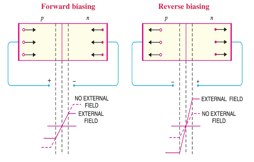
If an external potential of V volts is applied across the \(p-n\) junction such that the positive terminal is connected to the \(n\)-type material and the negative terminal is connected to the \(p\)-type material, as shown in the figure, the number of uncovered positive ions in the depletion region of the \(n\)-type material will increase due to the large number of free electrons drawn to the positive potential of the applied voltage. For similar reasons, the number of uncovered negative ions will increase in the \(p\)-type material. The net effect, therefore, is a widening of the depletion region. This widening of the depletion region will establish too great a barrier for the majority of carriers to overcome, effectively reducing the majority carrier flow to zero.
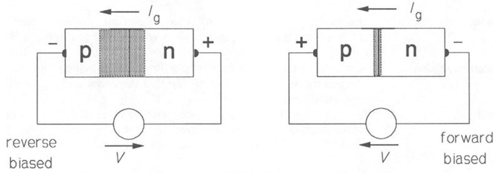
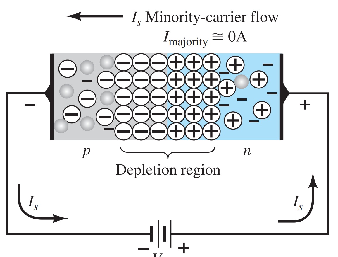
The number of minority carriers, however, entering the depletion region will not change, resulting in minority-carrier flow vectors of the same magnitude indicated in Fig. with no applied voltage.
The current that exists under reverse-bias conditions is called the reverse saturation current and is represented by \(I_{s}\).
The term saturation comes from the fact that it reaches its maximum level quickly and does not change significantly with increases in the reverse bias potential
Forward-Bias Condition
\(V_{D} \gt 0\) \(V\)
A forward bias or on condition is established by applying the positive potential to the \(p\)-type material and the negative potential to the \(n\)-type material, as shown in Fig.
The application of a forward-bias potential \(V_D\) will pressure electrons in the \(n\)-type material and holes in the \(p\)-type material to recombine with the ions near the boundary and reduce the width of the depletion region, as shown in Fig. The resulting minority-carrier flow of electrons from the \(p\)-type material to the \(n\)-type material (and of holes from the \(n\)-type material to the \(p\)-type material) has not changed in magnitude (since the conduction level is controlled primarily by the limited number of impurities in the material), but the reduction in the width of the depletion region has resulted in a heavy majority flow across the junction. An electron of the \(n\)-type material now sees a reduced barrier at the junction due to the reduced depletion region and a strong attraction for the positive potential applied to the \(p\)-type material. As the applied bias increases in magnitude, the depletion region will continue to decrease in width until a flood of electrons can pass through the junction, resulting in an exponential rise in current, as shown in the forward-bias region of the characteristics.
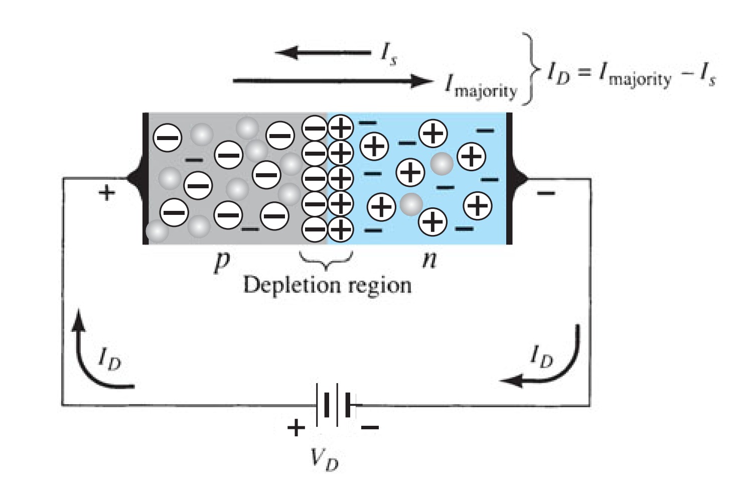
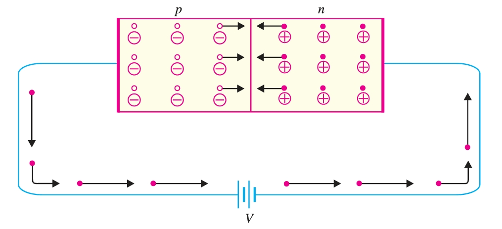
The mechanism of current flow in a forward biased \(pn\) junction can be summed up as under:
- (i) The free electrons from the negative terminal continue to pour into the \(n\)-region while the free electrons in the \(n\)-region move towards the junction.
- (ii) The electrons travel through the \(n\)-region as free-electrons i.e. current in \(n\)-region is by free electrons
- (iii) When these electrons reach the junction, they combine with holes and become valence electrons.
- (iv) The electrons travel through \(p\)-region as valence electrons i.e. current in the \(p\)-region is by holes.
- (v) When these valence electrons reach the left end of crystal, they flow into the positive terminal of the battery.
The current is carried by free electrons in \(n\)-type region whereas it is carried by holes in \(p\)-type region. However, the current is carried by free electrons in the external connecting wires.