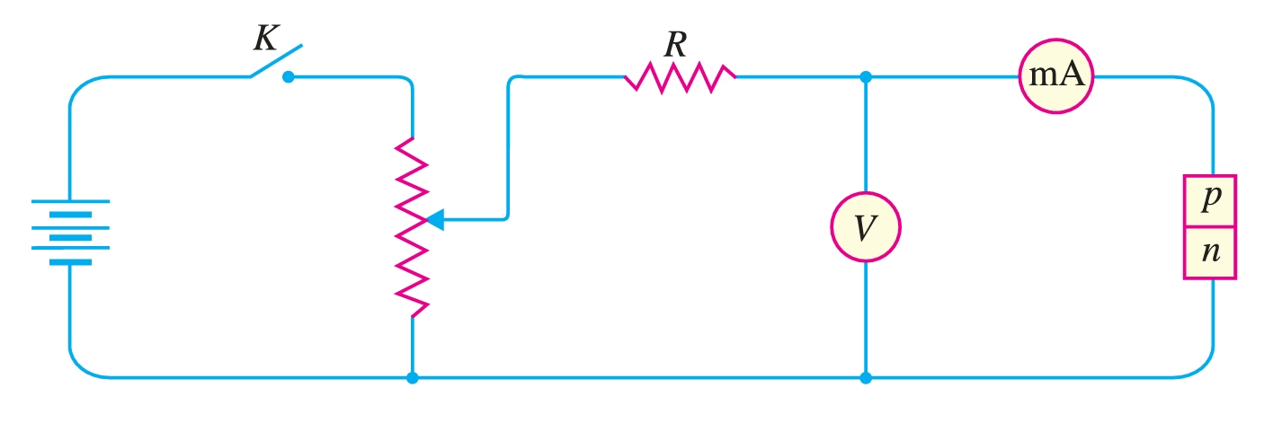
Volt-Ampere Characteristics
Volt-ampere or \(V-I\) characteristic of a \(pn\) junction (also called a semiconductor diode) is the curve between voltage across the junction and the circuit current. Usually, voltage is taken along \(x\)-axis and current along \(y\)-axis. Fig. shows the circuit arrangement for determining the \(V-I\) characteristics of a \(pn\) junction. The characteristics can be studied under three heads, namely; zero external voltage, forward bias and reverse bias.
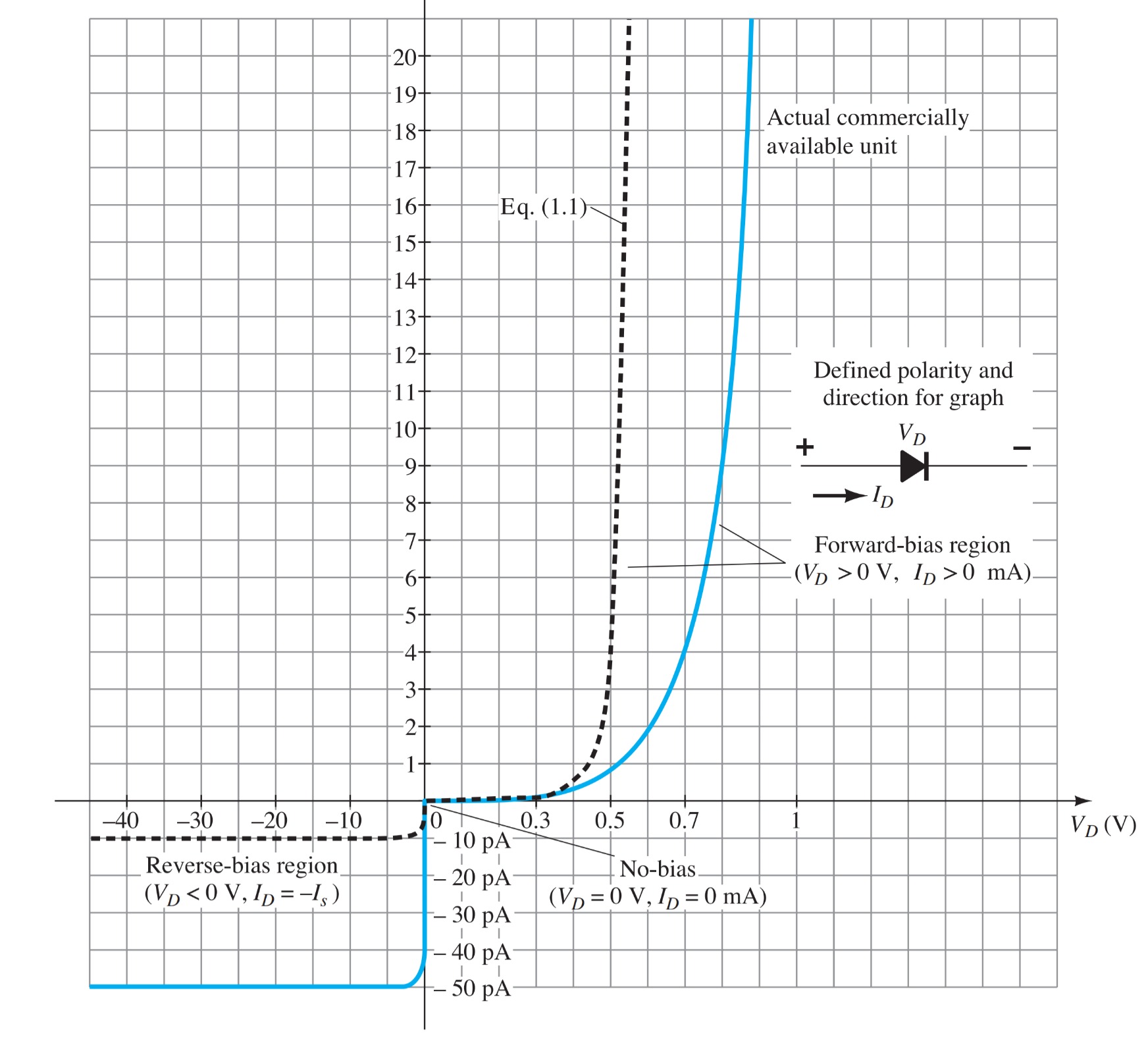
The general characteristics of a semiconductor diode can be defined by the following equation, referred to as Shockley’s equation, for the forward- and reverse-bias regions:
\[I_{D} = I_{s}(e^{V_{D}/\eta V_T} - 1)~(A)\]
where \(I_s\) is the reverse saturation current \(V_{D}\) is the applied forward-bias voltage across the diode \(\eta\) is an ideality factor, which is a function of the operating conditions and physical construction; it has a range between \(1\) and \(2\) depending on a wide variety of factors. The ideality factor, \( \eta=1\) for \(Ge\) and \(\eta=2\) for \(Si\) for relatively low levels of diode current (at or below the knee of the curve). The \( \eta=1\) for \(Ge\) and \(Si\) for higher levels of diode current (in the rapidly increasing section of the curve).
The voltage \(V_T\) in Eq. is called the thermal voltage and is determined by
\[V_T = \frac{k_B T_{K}}{q}~(V)\]
where \(k_B\) is Boltzmann's constant \(1.38 \times 10^{-23}\) \(J/K\)
\(T_K\) is the absolute temperature in kelvins \(273\) \(K\) the temperature in \(°C\)
\(q\) is the magnitude of electronic charge \(1.6 \times 10^{-19}\) \(C\)
If we expand the equation of each region:
\[I_{D} = I_{s}e^{V_{D}/\eta V_T} - I_{s}~~(A)\]
For positive values of \(V_{D}\), the first term of the above equation will grow very quickly and totally overpower the effect of the second term. The result is the following equation, which only has positive values and takes on the exponential format \(e^{x}\).
\[I_{D} = I_{s}(e^{V_{D}/\eta V_T})~~~[V_{D}~positive]\]
For negative values of \(V_D\), the exponential term drops very quickly below the level of \(I\), and the resulting equation for \(I_{D}\) is simply
\[I_{D} = -I_{s} ~~~[V_{D}~negative]\]
For negative values of \(V_{D}\), the current is essentially horizontal at the level of \(-I_{s}\).
The actual reverse saturation current of a commercially available diode will normally be measurably larger than that appearing as the reverse saturation current in Shockley’s equation.
This increase in level is due to a wide range of factors that include
- leakage currents
- generation of carriers in the depletion region
- higher doping levels that result in increased levels of reverse current
- sensitivity to the intrinsic level of carriers in the component materials by a squared factor—double the intrinsic level, and the contribution to the reverse current could increase by a factor of four.
- a direct relationship with the junction area—double the area of the junction and the contribution to the reverse current could double. High-power devices that have larger junction areas typically have much higher levels of reverse current.
- Temperature sensitivity—For every \(5\) \(°C\) increase in current, the level of reverse saturation current will double, whereas a \(10\) \(°C\) increase in current will result in a doubling of the actual reverse current of a diode.
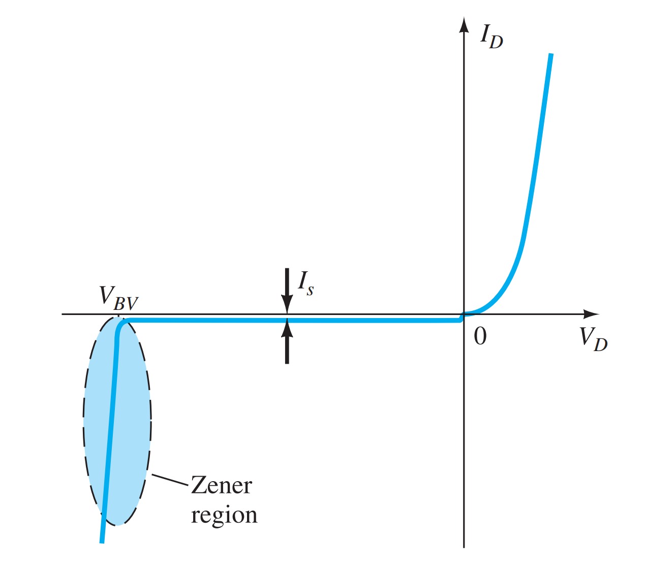
Breakdown Region
Even though the scale of Fig. is in tens of volts in the negative region, there is a point where the application of too negative a voltage with the reverse polarity will result in a sharp change in the characteristics, as shown in Fig. The current increases at a very rapid rate in a direction opposite to that of the positive voltage region. The reverse bias potential that results in this dramatic change in characteristics is called the breakdown potential and is given the label \(V_{BV}\).
Avalanche breakdown
As the voltage across the diode increases in the reverse-bias region, the velocity of the minority carriers responsible for the reverse saturation current \(I_{s}\) will also increase. Eventually, their velocity and associated kinetic energy \((W_K= \frac{1}{2}mv^2)\) will be sufficient to release additional carriers through collisions with otherwise stable atomic structures. That is, an ionization process will result whereby valence electrons absorb sufficient energy to leave the parent atom. These additional carriers can then aid the ionization process to the point where a high avalanche current is established, and the avalanche breakdown region is determined.
Zener breakdown
The avalanche region \((V_{BV})\) can be brought closer to the vertical axis by increasing the doping levels in the \(p\)- and \(n\)-type materials. However, as \(V_{BV}\) decreases to very low levels, such as \(5\) \(V\), another mechanism, called Zener breakdown, will contribute to the sharp change in the characteristic. It occurs because there is a strong electric field in the region of the junction that can disrupt the bonding forces within the atom and “generate” carriers. Although the Zener breakdown mechanism is a significant contributor only at lower levels of \(V_{BV}\), this sharp change in the characteristic at any level is called the Zener region, and diodes employing this unique portion of the characteristic of a \(p–n\) junction are called Zener diodes.
The breakdown region of the semiconductor diode described must be avoided if the response of a system is not to be completely altered by the sharp change in characteristics in this reverse-voltage region. The maximum reverse-bias potential that can be applied before entering the breakdown region is called the peak inverse voltage (referred to simply as the \(PIV\) rating) or the peak reverse voltage (denoted the \(PRV\) rating).
If an application requires a PIV rating more significant than that of a single unit, several diodes of the same characteristics can be connected in series. Diodes are also connected in parallel to increase the current-carrying capacity.
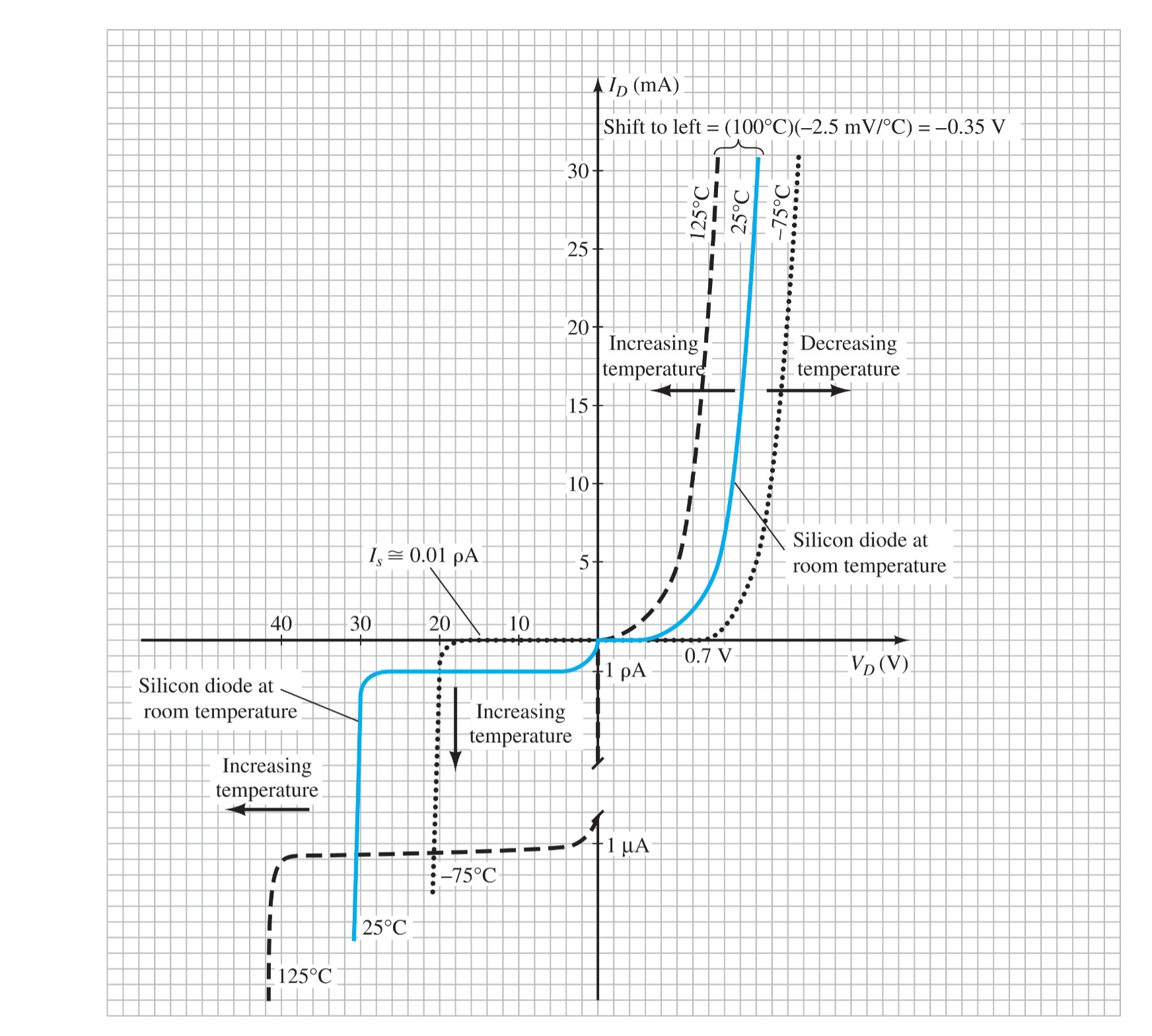
Temperature Effects
Temperature can have a marked effect on the characteristics of a semiconductor diode, as demonstrated by the characteristics of a silicon diode.
- In the forward-bias region, the characteristics of a silicon diode shift to the left at a rate of 2.5 mV per centigrade degree increase in temperature.
- In the reverse-bias region, the reverse current of a silicon diode doubles for every 10°C rise in temperature.
- The reverse breakdown voltage of a semiconductor diode will increase or decrease with temperature.
Silicon versus Germanium
Silicon diodes have, in general, higher PIV and current rating and wider temperature ranges than germanium diodes. PIV ratings for silicon can be in the neighborhood of 1000 V, whereas the maximum value for germanium is closer to 400 V. Silicon can be used for applications in which the temperature may rise to about 200°C (400°F), whereas germanium has a much lower maximum rating (100°C). The disadvantage of silicon as compared to germanium, as is the higher forward-bias voltage required to reach the region of upward swing. It is typically of the order of magnitude of 0.7 V for commercially available silicon diodes and 0.3 V for germanium diodes when rounded off to the nearest tenths. The increased offset for silicon is due primarily to the \(\eta\) factor. This factor plays a part in determining the shape of the curve only at very low current levels. Once the curve starts its vertical rise, the \(\eta\) factor drops to 1 (the continuous value for germanium). This is evidenced by the similarities in the curves once the offset potential is reached.
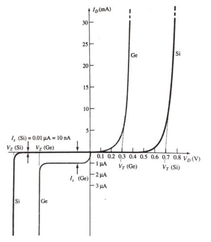
The threshold potential for Silicon (Si) and Germanium (Ge) is
\[V_{T} = 0.7 ~\text{Volts} ~(\text{Si})\] \[V_{T} = 0.3 ~\text{Volts} ~(\text{Ge})\]
Typical values of saturation current, \(I_{s}\) for silicon are much lower than that of germanium for similar power and current levels and even at high temperatures the levels of \(I_{s}\) for silicon diodes do not reach the same high levels obtained for germanium.
Limitations of pn junction
Every \(p-n\) junction has limiting values of maximum forward current, peak inverse voltage and maximum power rating. The \(p-n\) junction will give satisfactory performance if it is operated within these limiting values. However, if these values are exceeded, the \(p-n\) junction may be destroyed due to excessive heat.
(i) Maximum forward current
Maximum forward current is the highest instantaneous forward current that a \(p-n\) junction can conduct without damage to the junction. Manufacturer’s data sheet usually specifies this rating. If the forward current in a \(p-n\) junction is more than this rating, the junction will be destroyed due to overheating.
(ii) Peak inverse voltage (PIV)
Peak inverse voltage is the maximum reverse voltage that can be applied to the \(p-n\) junction without damage to the junction. If the reverse voltage across the junction exceeds its PIV, the junction may be destroyed due to excessive heat. The peak inverse voltage is of particular importance in rectifier service. A \(p-n\) junction diode is used as a rectifier to change alternating current into direct current. In such applications, the reverse voltage across the diode during negative half-cycle of a.c. does not exceed the PIV of diode.
(iii) Maximum power rating
Maximum power rating is the maximum power that can be dissipated at the junction without damaging it. The power dissipated at the junction is equal to the product of junction current and the voltage across the junction. This is a very important consideration and is invariably specified by the manufacturer in the data sheet.