Diode Resistance
The resistance of the diode will also change due to the nonlinear shape of the characteristic curve as the operating point of a diode moves from one region to another. A forward-biased diode conducts easily, whereas a reverse-biased diode practically conducts no current. This means that the forward resistance of a diode is much lower than its reverse resistance.
Forward resistance.
The resistance offered by the diode to forward bias is known as forward resistance. This resistance is not the same for the flow of direct current as for the alternating current. Accordingly, this resistance is of two types, namely, d.c. forward resistance (Static Resistance) and a.c. forward resistance (Dynamic Impedance).
Static Resistance (D.C. Resistance)
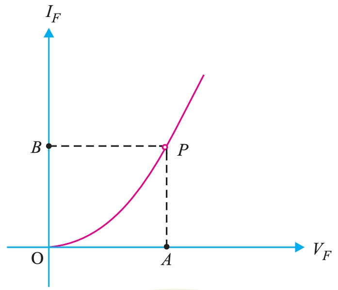
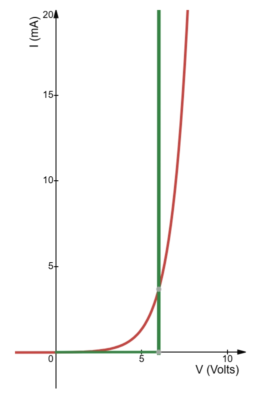
Applying a DC voltage to a circuit containing a semiconductor diode results in an operating point on the characteristic curve that remains constant over time. The resistance of the diode at the operating point can be found simply by finding the corresponding levels of \(V_D\) and \(I_D\) as shown in Fig. 1, and applying the following equation:
\[R_{D} = \frac{V_{D}}{I_{D}}\]
The dc resistance levels at the knee and below will be greater than the resistance levels obtained for the vertical rise section of the characteristics, i.e., the lower the current through a diode, the higher the dc resistance level. The DC resistance of a diode is independent of the shape of the characteristic in the region surrounding the point of interest.
The DC resistance levels for the diode
| \(V_{D}\) | \(I_{D}\) | \(R_{D}\) |
|---|---|---|
| 0.5 V | 2 \(mA\) | 250 \(\Omega\) |
| 0.8 V | 20 \(mA\) | 40 \(\Omega\) |
| 10 V | 1 \(\mu A\) | 10 \(M\Omega\) |
Dynamic Resistance (A.C. Impedance)
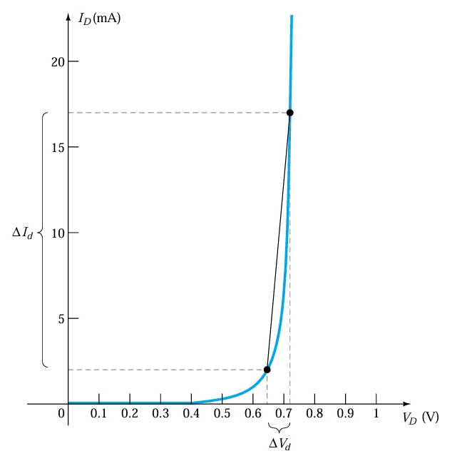
A sinusoidal voltage applied to the input varies the input and moves the instantaneous operating point up and down along the characteristics, thus defining a specific change in current and voltage; hence, the resistance also changes accordingly.
A straight line drawn tangent to the curve through the \(Q\)-point as shown in Fig. 2 will define a particular change in voltage and current that can be used to determine the acor dynamic resistance for this region of the diode characteristics. An effort should be made to keep the change in voltage and current as small as possible and to keep them equidistant from the Q-point. In equation form,
\[r_{d} = \frac{\Delta V_{d}}{I_{d}}\]
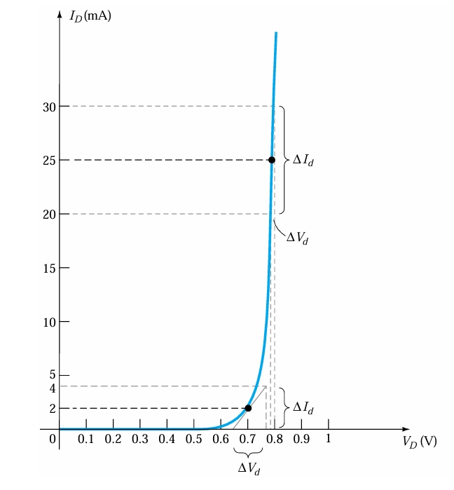
The steeper the slope, the less the value of \(V_{d}\) for the same change in \(I_{d}\) and the less the resistance. The ac resistance in the vertical-rise region of the characteristic is therefore quite small, while the ac resistance is much higher at low current levels.
The dynamic resistance levels for the diode
| \(V_{1}\) | \(V_{2}\) | \(I_{1}\) | \(I_{2}\) | \(V_{d}\) | \(I_{d}\) | \(r_{d}\) | \(R_{D} = \frac{V_{1}+V_{1}}{I_{1}+I_{2}}\) |
|---|---|---|---|---|---|---|---|
| 0.65 V | 0.75 V | 0 \(mA\) | 4 \(mA\) | 0.11 V | 4 \(mA\) | 27.5 \(\Omega\) | 350 \(\Omega\) |
| .78 V | 0.80 V | 20 \(mA\) | 30 \(mA\) | 0.02 V | 10 \(mA\) | 2 \(\Omega\) | 31.62 \(\Omega\) |
The dynamic resistance is defined as the The derivative of a function at a point is equal to the slope of the tangent line drawn at that point.
We can derive the dynamic resistance from the diode equation as follows:
\[I_D = [I_s (e^{(\eta V_D/V_T)}-1)]\]
Taking the derivative of the above equation with respect to the applied bias (\(V_D\)) will result in
\[\frac{d}{d V_D}(I_D) = \frac{d}{d V}[I_s (e^{(\eta V_D/V_T)}-1)]\]
\[\frac{d I_D}{d V_D} = I_s e^{(\eta V_D/V_T)}\left(\frac{\eta}{V_T}\right)\] \[ \frac{d I_D}{d V_D} = \frac{\eta}{V_T}(I_D + I_s)\]
But, \(I_D \gg I_s\) in the forward characteristic of a \(p-n\) junction diode, hence, we can ignore \(I_s\), and the equation becomes
\[\frac{d I_D}{d V_D} \cong \left(\frac{\eta}{V_T}\right) I_D \]
Substituting \(\eta = 1\) for \(Ge\) and \(Si\) in the vertical-rise section of the forward characteristics, we get, \(V_T\) as
\[V_T = \frac{k_B T}{e} = \frac{1.38 \times 10^{-23} \times T}{1.6 \times 10^{-19}} = \left(\frac{T}{11600}\right)\]
Hence,
\[\frac{d I_D}{d V_D} = \left(\frac{11600}{T}\right) I_D \]
and at room temperature, 298 K, we get,
\[\frac{d I_D}{d V_D} = \left(\frac{11600}{298}\right) I_D \cong 38.93 ~I_D\]
Then the dynamic resistance is obtained by taking the inverse of the above equation, so we get
\[r_d = \frac{d V_D}{d I_D} = \frac{1}{38.93 ~I_D} \]
or
\[r_d = \frac{26 ~mV}{I_D}\bigg|_{\text{Ge, Si}}\]
It implies that the dynamic resistance can be found simply by substituting the operating current of the diode into the equation. For lesser values of \(I_{D}\), \(\eta = 2\), and the value of \(r_d\) obtained must be multiplied by a factor of 2. For small values of \(I_{D}\) below the knee of the curve, the above equation of dynamic resistance becomes inappropriate.
All the resistance levels determined thus far have been defined by the \(p-n\) junction and do not include the resistance of the semiconductor material itself (called body resistance) and the resistance introduced by the connection between the semiconductor material and the external metallic conductor (called contact resistance). These additional resistance levels can be included in \(r_d\) by adding resistance denoted by \(r_B\). The resistance \(r_d\), therefore, includes the dynamic resistance and the resistance \(r_B\).
\[r'_d = \left[\frac{26 ~mV}{I_D}\right] + r_B ~~~\Omega\]
Average AC resistance
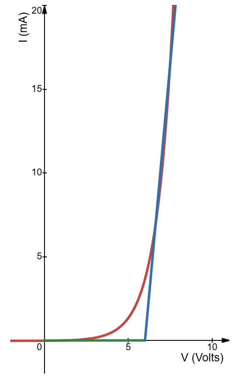
If the input signal is sufficiently large to produce a broad swing (Figure 3), the resistance associated with the device for this region is called the average ac resistance. The average ac resistance is, by definition, the resistance determined by a straight line drawn between the two intersections established by the maximum and minimum values of input voltage
\[r_{av} = \frac{d V_D}{d I_D}\bigg|_{\text{point to point}} \]
Reverse resistance.
The resistance offered by the diode to the reverse bias is known as reverse resistance. The resistance levels in the reverse-bias region will naturally be quite high. It can be d.c. reverse resistance or a.c. reverse resistance depending on whether the reverse bias is direct or changing. Ideally, the reverse resistance of a diode is infinite. However, in practice, the reverse resistance is not infinite because for any value of reverse bias, there does exist a small leakage current. It may be emphasised that reverse resistance is much larger than forward resistance. In germanium diodes, the ratio of reverse to forward resistance is 40000 : 1, while for silicon, this ratio is 1000000 : 1.
Diode equivalent circuits
An equivalent circuit is a combination of elements properly chosen to best represent the actual terminal characteristics of a device, system, or such in a particular operating region.
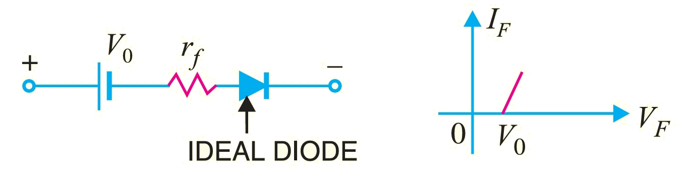
Piecewise-Linear Equivalent Circuit
An equivalent circuit for a diode is to approximate the characteristics of the device by straight-line segments, and the resulting segments are sufficiently close to the actual curve to establish an equivalent circuit that will provide an excellent first approximation to the actual behavior of the device. It defines the resistance level of the device when it is in the ON state. The ideal diode is included to ensure that conduction occurs in only one direction through the device, and that a reverse-bias condition results in the device being in an open-circuit state. Since a silicon semiconductor diode does not reach the conduction state until \(V_D\) reaches 0.7 V with a forward bias, a battery \(V_T\) opposing the conduction direction must appear in the equivalent circuit. The battery simply specifies that the voltage across the device must be greater than the threshold battery voltage before conduction through the device in the direction dictated by the ideal diode can be established. When conduction is established, the resistance of the diode will be the specified value of \(r_{av}\).
Simplified Equivalent Circuit
For most applications, the resistance \(r_{av}\) is sufficiently small to be ignored in comparison to the other elements of the network.
\[R_{network} \gg r_{av}\]
The removal of \(r_{av}\) from the equivalent circuit is the same as implying that the characteristics of the diode. It states that a forward-biased silicon diode is used in an electronic system. Under DC conditions, it has a drop of 0.7 V across it in the conduction state at any diode current level.
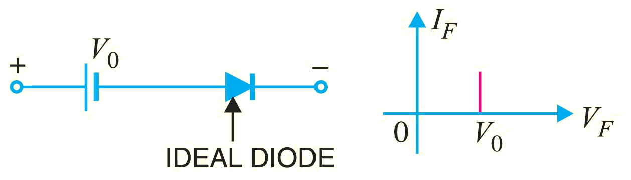
Ideal Equivalent Circuit
Now that \(r_{av}\) has been removed from the equivalent circuit, it is established that a 0.7 V level can often be ignored in comparison to the applied voltage level. In this case, the equivalent circuit reduces to that of an ideal diode.
\[R_{network} \gg r_{av} \]
\[E_{network} \gg V_T\]