Zener Diode
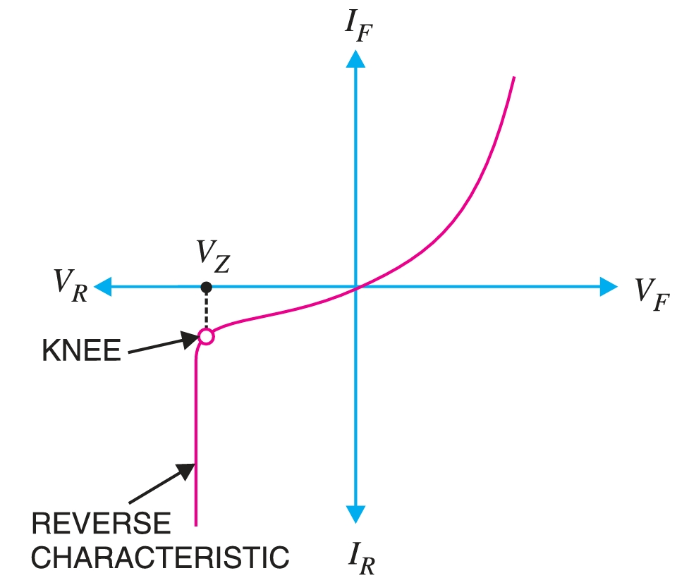
A zener diode is a special type of diode that is designed to operate in the reverse breakdown region. An ordinary diode operated in this region will usually be destroyed due to excessive current. This is not the case for the zener diode. A zener diode is heavily doped to reduce the reverse breakdown voltage. This causes a very thin depletion layer. As a result, a zener diode has a sharp reverse breakdown voltage \(V_{Z}\). This is clear from the reverse characteristic of zener diode.
The reverse characteristic drops in an almost vertical manner at reverse voltage \(V_{Z}\). As the curve reveals, two things happen when \(V_{Z}\) is reached :
- (i) The diode current increases rapidly.
- (ii) The reverse voltage \(V_{Z}\) across the diode remains almost constant.
In other words, the zener diode operated in this region will have a relatively constant voltage across it, regardless of the value of current through the device. This permits the zener diode to be used as a voltage regulator.
When the reverse bias on a \(p-n\) diode is increased, a critical voltage, called the breakdown voltage, is reached, where the reverse current increases sharply to a high value. The breakdown region is the knee of the reverse characteristic, as shown in Fig. 1.
The satisfactory explanation of this breakdown of the junction was first given by the American scientist C. Zener. Therefore, the breakdown voltage is sometimes called zener voltage and the sudden increase in current is known as zener current. The breakdown or zener voltage depends upon the amount of doping. If the diode is heavily doped, the depletion layer will be thin, and the breakdown of the junction will occur at a lower reverse voltage; such a diode is known as a zener diode. On the other hand, a lightly doped diode has a higher breakdown voltage.
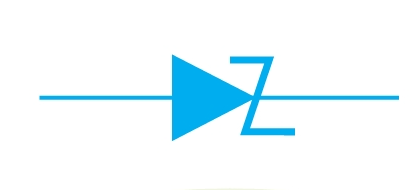
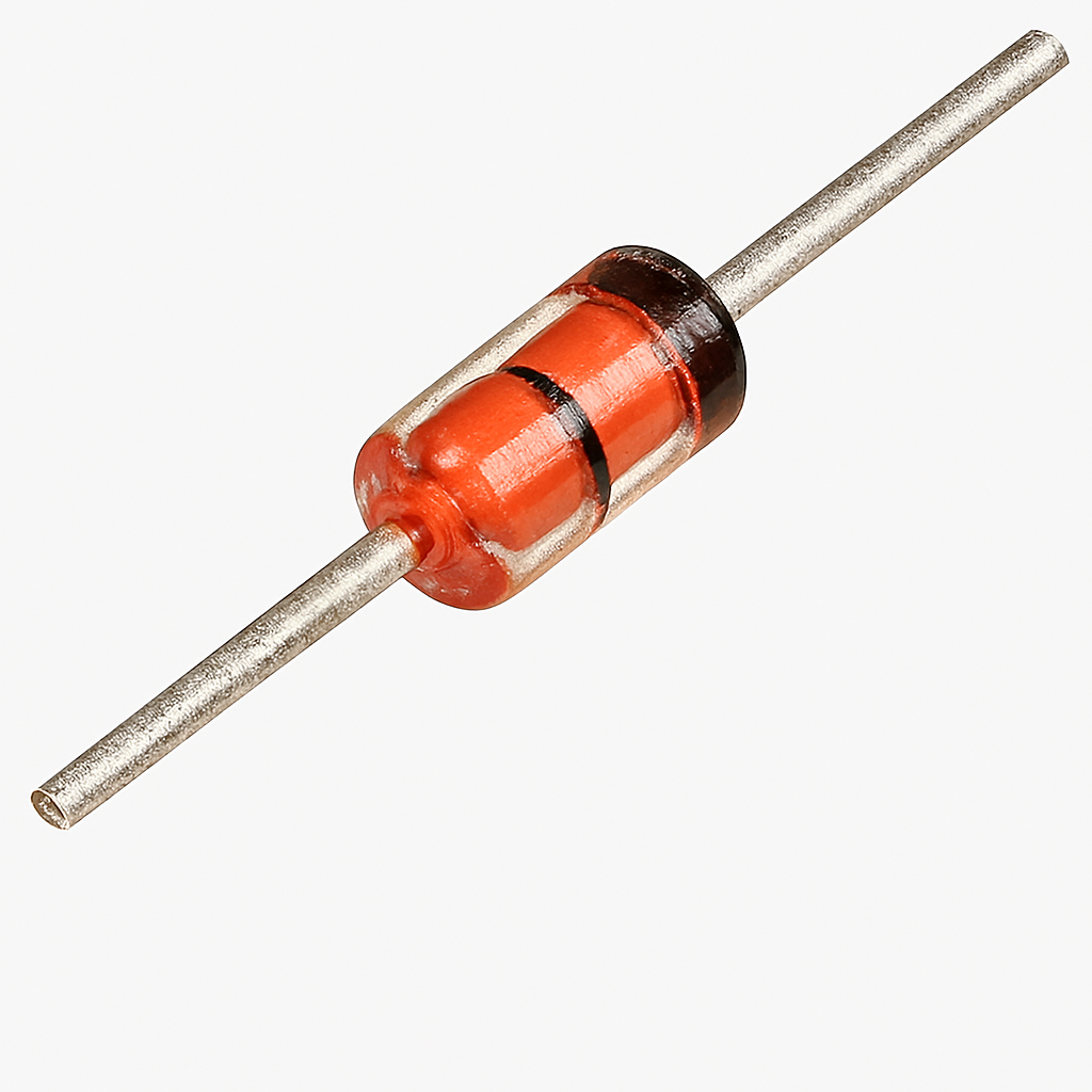
A properly doped crystal diode that has a sharp breakdown voltage is known as a zener diode. Fig. 2 shows the symbol of a zener diode. It appears to be just like an ordinary diode, except that the bar is bent into a Z-shape. The following points may be noted about the Zener diode:
- (i) A zener diode is like an ordinary diode except that it is properly doped so as to have a sharp breakdown voltage.
- (ii) A zener diode is always reverse connected, i.e., it is always reverse-biased.
- (iii) A zener diode has a sharp breakdown voltage, called zener voltage, \(V_Z\).
- (iv) When forward-biased, its characteristics are just those of an ordinary diode.
- (v) The zener diode is not immediately burnt just because it has entered the breakdown region. As long as the external circuit connected to the diode limits the diode current to less than the burnout value, the diode will not burn out.
Zener Diode as Voltage Stabiliser
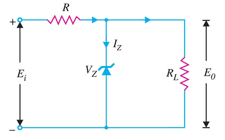
A zener diode can be used as a voltage regulator to provide a constant voltage from a source whose voltage may vary over a sufficient range. The circuit arrangement is shown in Fig. 3. The zener diode with zener voltage \(V_Z\) is reverse-biased across the load \(R_L\), across which a constant output is desired. The series resistance \(R\) absorbs the output voltage fluctuations, maintaining a constant voltage across the load. It may be noted that the zener will maintain a constant voltage \(V_Z (= E_0)\) across the load so long as the input voltage does not fall below \(V_Z\).
When the circuit is properly designed, the load voltage \(E_0\) remains essentially constant (equal to \(V_Z\)) even as the input voltage \(E_i\) and load resistance \(R_L\) vary widely.
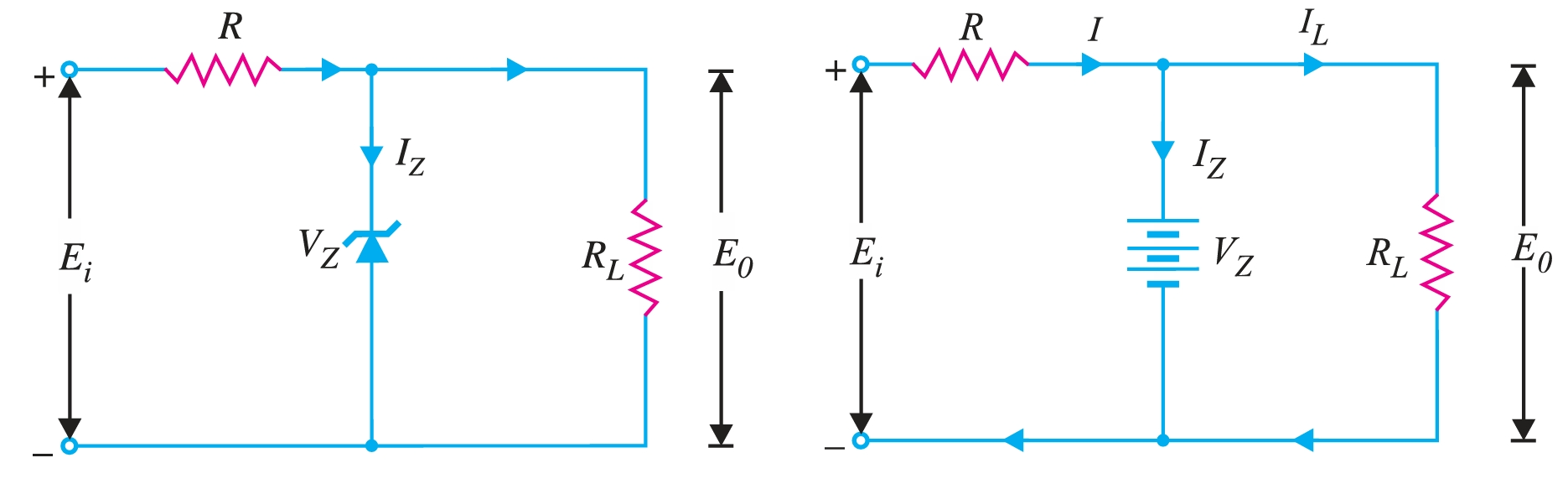
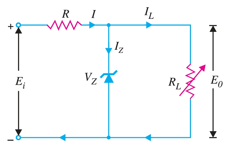
- (i) Suppose the input voltage increases. Since the zener is in the breakdown region, the zener diode is equivalent to a battery with voltage \(V_Z\), as shown in Fig. 3. It is clear that the output voltage remains constant at \(V_Z (= E_0)\). The excess voltage is dropped across the series resistance R, which increases the total current \(I\). The zener will conduct the increase of current \(I\) while the load current remains constant. Hence, output voltage \(E_0\) remains constant irrespective of the changes in the input voltage \(E_i\).
- (ii) Now suppose that the input voltage is constant, but the load resistance \(R_L\) decreases. This will increase the load current. The extra current cannot come from the source because a drop in \(R\) (and hence source current \(I\)) will not change as the zener is within its regulating range. The additional load current will come from a decrease in zener current \(I_Z\). Consequently, the output voltage remains constant.
\[\text{Voltage drop across } R = E_i − E_0\] \[\text{Current through R, } I = I_Z + I_L\] Applying Ohm’s law, we have,
\[R = \frac{E_i − E_0}{I_Z + I_L}\]
The analysis of Zener diode circuits is quite similar to that applied to the analysis of semiconductor diodes. The first step is to determine the state of the zener diode, i.e., whether the zener is in the ON state or OFF state. Next, the zener is replaced by its appropriate model. Finally, the unknown quantities are determined from the resulting circuit.
Fixed Input Voltage and Load Resistance
This is the simplest case, shown in Fig. 4. Here, the applied voltage \(E_i\) and the load \(R_L\) are fixed. The first step is to find the state of the Zener diode. This can be determined by removing the zener from the circuit and calculating the voltage \(V\) across the resulting open circuit.
\[V = E_0 = \frac{R_L E_i}{R + R_L}\]
If \(V \geq V_Z\), the zener diode is in the ON state and its equivalent model can be substituted as shown in Fig. 2. If \(V < V_Z\), the diode is in the OFF state.
- (i) On state \[E_0 = V_Z \] \[I_Z = I - I_L \quad\text{where,}\quad I_L = \frac{E_0}{R_L} \quad\text{and}\quad I = \frac{E_i-E_0}{R}\] \[\text{Power dissipated in Zener, } P_Z = V_Z I_Z\]
- (ii) Off state \[I = I_L \text{ and } I_Z = 0\] \[V_R = E_i − E_0 \quad\text{and}\quad V = E_0 \quad (V < V_Z)\] \[\therefore P_Z = V I_Z = V \times 0 = 0\]
Fixed Input Voltage and Variable Load resistance.
This case is shown in Fig. 4. Here, the applied voltage (\(E_i\)) is fixed while the load resistance \(R_L\) (and hence the load current \(I_L\)) changes. Note that there is a definite range of \(R_L\) values (and hence \(I_L\) values) which will ensure the zener diode to be in ON state. Let us calculate that range of values.
- (i) \(R_{L\text{min}}\) and \(I_{L\text{max}}\)
Once the zener is in the ON state, load voltage \(E_0 (= V_Z)\) is constant. As a result, when load resistance is minimum (i.e., \(R_{L\text{min}}\)), load current will be maximum (\(I_L = E_0/R_L\)). In order to find the minimum load resistance that will turn the zener on, we simply calculate the value of \(R_L\) that will result in \(E_0 = V_Z\), i.e., \[E_0 = V_Z = \frac{R_L E_i}{R + R_L}\] \[ V_Z (R + R_L) = R_L E_i\] \[ V_Z R + V_Z R_L = R_L E_i\] \[ V_Z R = R_L E_i - V_Z R_L\] \[ V_Z R = R_L (E_i - V_Z)\] \[R_L = \frac{V_Z R}{E_i - V_Z}\] Hence, \(R_{L\text{min}}\) is obtained as: \[\therefore\quad R_{L\text{min}} = \frac{R V_Z}{E_i - V_Z}\] This is the minimum load resistance required to ensure the zener is in the ON state. Any load resistance below this value will result in a voltage \(E_{0}\) across the load less than \(V_{Z}\), and the zener will be in the OFF state. \[\text {Clearly;}\qquad\qquad I_{L\text{max}} = \frac{E_0}{R_{L\text{min}}} = \frac{V_Z}{R_{L\text{min}}}\] - (ii) \(I_{L\text{min}}\) and \(R_{L\text{max}}\) It is easy to see that when the load resistance is maximum, the load current is \(L_{min}\). Now, \[\text{Zener current, } I_Z = I − I_L\] When the zener is in the ON state, \(I\) remains fixed. That is, the Voltage across \(R\), \(V_R = E_i − E_0\) and \(I = V_R/R\). As \(E_i\) and \(E_0\) are fixed, \(I\) remains the same. This means that when \(I_L\) is maximum, \(I_Z\) will be minimum. On the other hand, when \(I_L\) is minimum, \(I_Z\) is maximum. If the maximum current that a zener can carry safely is \(I_{ZM}\), then \[I_L = I - I_{ZM}\] \[R_{L\text{max}} = \frac{E_0}{I_{L\text{min}}} = \frac{V_Z}{I_{L\text{min}}}\] If the load resistance exceeds this limiting value, the current through the zener will exceed \(I_{ZM}\) and the device may burn out.
Fixed load resistance and Variable input voltage.
This case is shown in Fig. 5. Here, the load resistance \(R_L\) is fixed while the applied voltage (\(E_i\)) changes. Note that there is a definite range of \(E_i\) values that will ensure that the zener diode is in the ON state. Let us calculate that range of values.
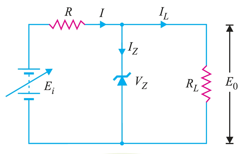
- (i) \(E_{i(\text{min})}\).
To determine the minimum applied voltage that will turn the zener on, simply calculate the value of \(E_i\) that will result in the load voltage, \(E_0 = V_Z\), i.e., \[E_0 = V_Z = \frac{R_L E_i}{R + R_L}\] \[\therefore \quad E_{i(\text{min})} = \frac{(R + R_L)V_Z}{R_L}\] - (ii) \(E_{i(\text{max})}\) Now, \[\text{current through } R, I = I_Z + I_L\] Since \(I_L (= E_0/R_L = V_Z/R_L)\) is fixed, the value of \(I\) will be maximum when zener current is maximum, i.e., \[I_{\text{max}} = I_{ZM} + I_L\] Now \[E_i= I R + E_0\] Since \(E_0 (= V_Z)\) is constant, the input voltage will be maximum when \(I\) is maximum. \[\therefore \quad E_{i(\text{max})} = I_{\text{max}} R + V_Z\] which means, \[\therefore \quad E_{i(\text{max})} = (I_{ZM} + I_L) R + V_Z\] \[\therefore \quad E_{i(\text{max})} = \left(I_{ZM} + \frac{V_Z}{R_L}\right) R + V_Z\]