Photo diode
A Photo diode is a reverse-biased silicon or germanium \(pn\) junction in which reverse current in creases when the junction is exposed to light. The reverse current in a photo diode is directly proportional to the intensity of light falling on its \(pn\) junction. This means that greater the intensity of light falling on the \(pn\) junction of photo diode, the greater will be the reverse current.
When a rectifier diode is reverse biased, it has a very small reverse leakage current. The same is true for a photo diode. The reverse current is produced by thermally generated electron hole pairs which are swept across the junction by the electric field created by the reverse voltage. In a rectifier diode, the reverse current increases with temperature due to an increase in the number of electron-hole pairs. A photo diode differs from a rectifier diode in that when its \(pn\) junction is exposed to light, the reverse current increases with the increase in light intensity and vice-versa.
This is explained as follows. When light (photons) falls on the \(pn\) junction, the energy is imparted by the photons to the atoms in the junction. This will create more free electrons (and more holes). This is true only if the light energy is applied at the junction. If it is applied to the crystal at some distance from the junction, the free electrons and holes will recombine (thus neutralising each other) before they can join the flow of reverse current. These additional free electrons will increase the reverse current.
As the intensity of light incident on the \(pn\)junction increases, the reverse current also increases. In other words, as the incident light intensity increases, the resistance of the device (photo diode) decreases. It is for this reason that semiconductor devices such as diodes and transistors are usually enclosed in opaque case to protect them from light. Those diodes or transistors which are used for light-detecting, on the other hand, must be encased in transparent plastic or glass so that light may fall on them.
Photo diode package.
Fig. 1 shows a typical photo diode package. It consists of a \(pn\) junction mounted on an insulated substrate and sealed inside a metal case. A glass window is mounted on top of the case to allow light to enter and strike the \(pn\) junction. The two leads extending from the case are labelled anode and cathode. The cathode is typically identified by a tab extending from the side of the case.
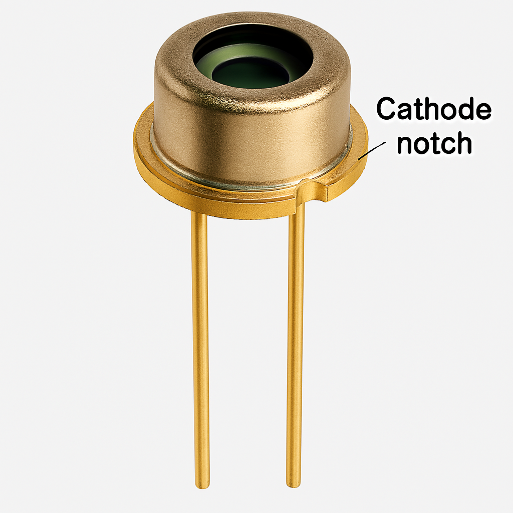
Fig. 2 shows the basic photo diode circuit. The circuit has reverse biased photo diode, resistor \(R\) and d.c. supply.
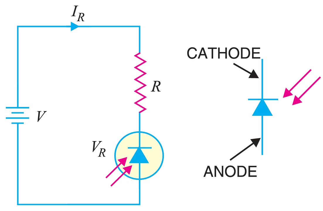
The operation of the photo diode is as under :
- (i) When no light is incident on the \(pn\) junction of photo diode, the reverse current \(I_R\) is extremely small. This is called dark current. The resistance of photo diode with no incident light is called dark resistance (R_R). Hence, the Dark resistance of photo diode is expressed as, \[R_R = \frac{V_R}{\text{Dark Current}}\]
- (ii) When light is incident on the \(pn\) junction of the photo diode, there is a transfer of energy from the incident light (photons) to the atoms in the junction. This will create more free electrons (and more holes). These additional free electrons will increase the reverse current.
- (iii) As the intensity of light increases, the reverse current \(I_R\) goes on increasing till it becomes maximum. This is called saturation current.
Characteristics of Photo diode
There are two important characteristics of photo diode.
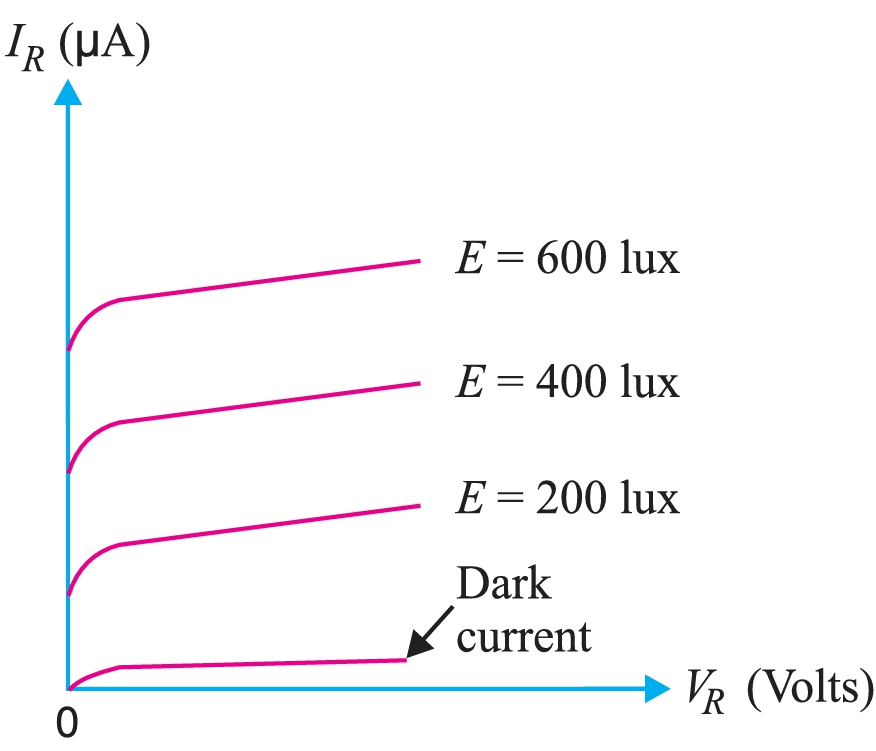
- (i) Reverse voltage-Reverse current curve. Fig. 3 shows the graph between reverse current (\(I_R\)) and reverse voltage (\(V_R\)) for various illumination levels. The reverse current \(I_R\) increases as the illumination (\(E\)) on the \(pn\) junction of photo diode is increased for a given reverse-biased voltage \(V_R\).
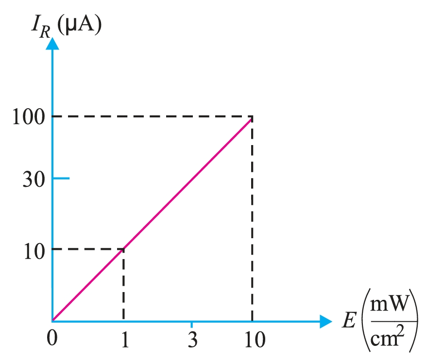
- (ii) Reverse current-Illumination curve. Fig. 4 shows the graph between reverse current (\(I_R\)) and illumination (\(E\)) of a photo diode. The reverse current is shown on the vertical axis and is measured in \(\mu A\). The illumination is indicated on the horizontal axis and is measured in \(mW/cm^{2}\). Note that graph is a straight line passing through the origin. \[\therefore I_R = m~E\]
where, \(m\) = slope of the straight line. The quantity \(m\) is called the sensitivity of the photo diode.
Applications of Photo diodes
There are a large number of applications of photo diodes. However, we shall give two applications of photo diodes by way of illustration.
Alarm circuit using Photo diode.
Light from a light source is allowed to fall on a photo diode fitted in the doorway. The reverse current \(I_R\) will continue to flow so long as the light beam is not broken. If a person passes through the door, light beam is broken and the reverse current drops to the dark current level. As a result, an alarm is sounded.
Counter circuit using photo diode
A photo diode may be used to count items on a conveyor belt. A source of light sends a concentrated beam of light across a conveyor to a photo diode. As the object passes, the light beam is broken, \(I_R\) drops to the dark current level and the count is increased by one.