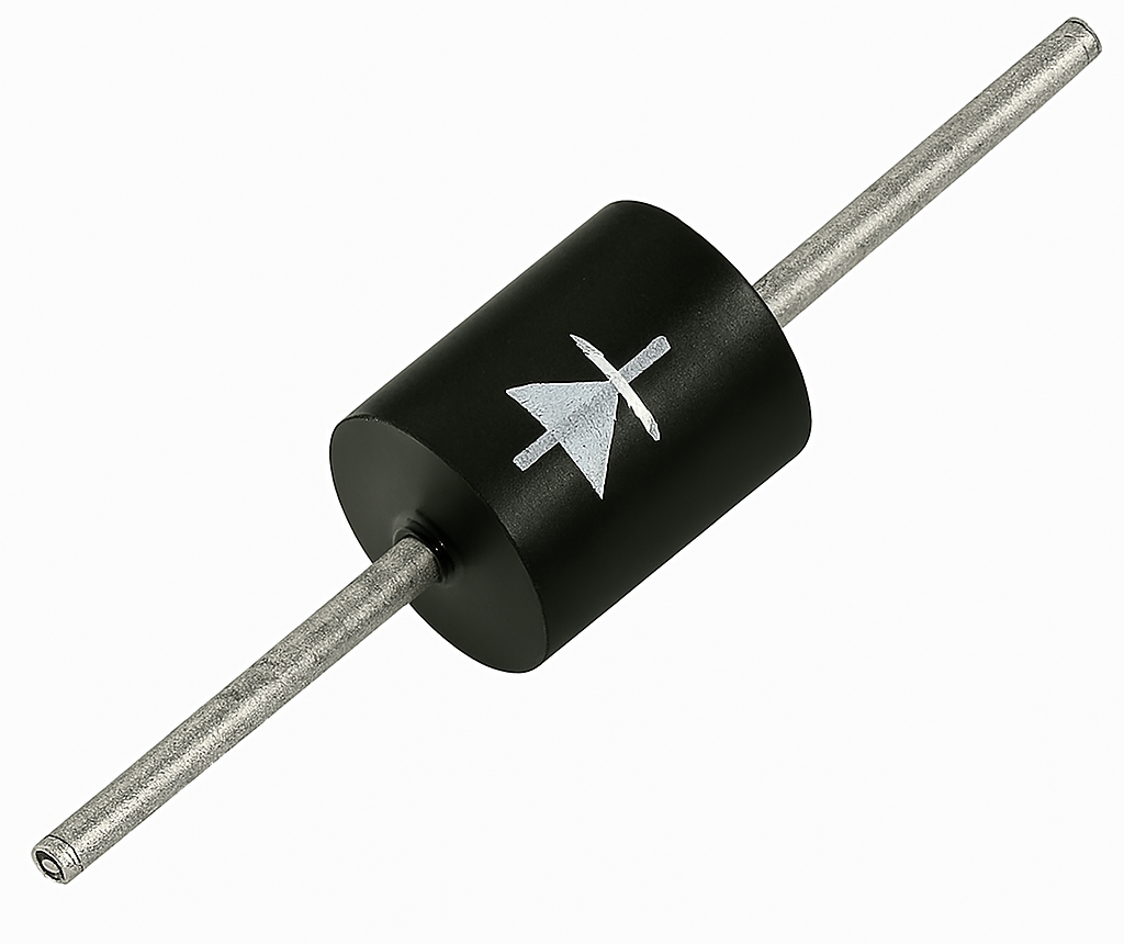
Tunnel Diode
A tunnel diode is a \(pn\) junction that exhibits negative resistance between two values of forward voltage (i.e., between peak-point voltage and valley-point voltage).
A conventional diode exhibits positive resistance when it is forward biased or reverse biased. However, if a semiconductor junction diode is heavily doped with impurities, it exhibits negative resistance (i.e. current decreases as the voltage is increased) in certain regions in the forward direc tion. Such a diode is called tunnel diode.
The tunnel diode is basically a \(pn\) junction with heavy doping of \(p\)-type and \(n\)-type semiconductor materials. In fact, a tunnel diode is doped approximately 1000 times as heavily as a conventional diode. This heavy doping results in a large number of majority carriers. Because of the large number of carriers, most are not used during the initial recombination that produces the deple tion layer. As a result, the depletion layer is very narrow. In comparison with conventional diode, the depletion layer of a tunnel diode is 100 times narrower. The operation of a tunnel diode depends upon the tunneling effect and hence the name.
The heavy doping provides a large number of majority carriers. Because of the large number of carriers, there is much drift activity in \(p\) and \(n\) sections. This causes many valence electrons to have their energy levels raised closer to the conduction region. Therefore, it takes only a very small applied forward voltage to cause conduction.
The movement of valence electrons from the valence energy band to the conduction band with little or no applied forward voltage is called tunneling. Valence electrons seem to tunnel through the forbidden energy band.
As the forward voltage is first increased, the diode current rises rapidly due to tunneling effect. Soon the tunneling effect is reduced and current flow starts to decrease as the forward voltage across the diode is increased. The tunnel diode is said to have entered the negative resistance region. As the voltage is further increased, the tunneling effect plays less and less part until a valley-point is reached. From now onwards, the tunnel diode behaves as ordinary diode i.e., diode current increases with the increase in forward voltage.
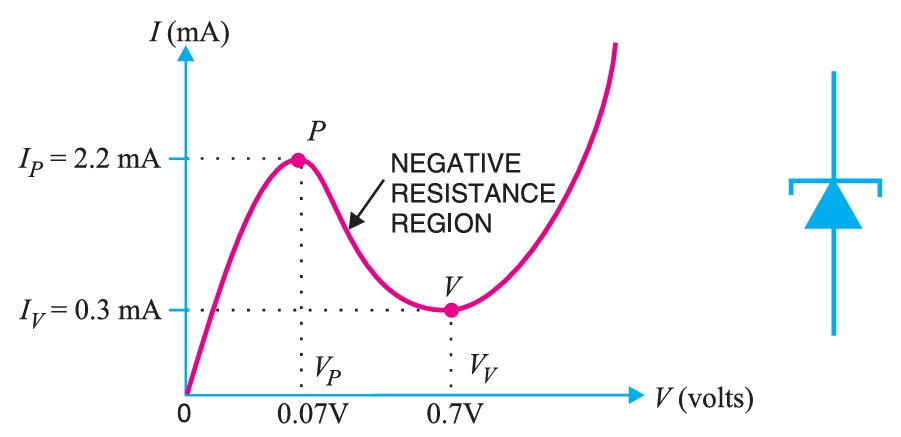
Fig. shows the \(V-I\) characteristic of a typical tunnel diode. As the forward voltage across the tunnel diode is increased from zero, electrons from the \(n\)- region tunnel through the potential barrier to the \(p\)-region. As the forward voltage increases, the diode current also increases until the peak-point \(P\) is reached. The diode current has now reached peak current \(I_P\) (\(= 2.2 ~mA\)) at about peak-point voltage \(V_P\) (\(= 0.07 ~V\)). Until now the diode has exhibited positive resistance.
As the voltage is increased beyond \(V_P\), the tunneling action starts decreasing and the diode current decreases as the forward voltage is increased until valley-point \(V\) is reached at valley-point voltage \(V_V\) (\(= 0.7 ~V\)). In the region between peak-point and valley-point (i.e., between points \(P\) and \(V\)), the diode exhibits negative resistance i.e., as the forward bias is increased, the current decreases. This suggests that tunnel diode, when operated in the negative resistance region, can be used as an oscillator or a switch.
When forward bias is increased beyond valley-point voltage \(V_V\) (\(= 0.7 ~V\)), the tunnel diode behaves as a normal diode. In other words, from point \(V\) onwards, the diode current increases with the increase in forward voltage i.e., the diode exhibits positive resistance once again. Fig. shows the symbol of tunnel diode. A tunnel diode has a high reverse current but operation under this condition is not generally used.
Varactor Diode
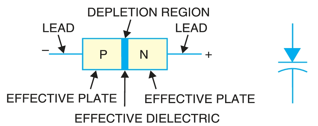
A junction diode which acts as a variable capacitor under changing reverse bias is known as a varactor diode.
When a \(pn\) junction is formed, depletion layer is created in the junction area. Since there are no charge carriers within the depletion zone, the zone acts as an insulator. The \(p\)-type material with holes (considered positive) as majority carriers and \(n\)-type material with electrons (−ve charge) as majority carriers act as charged plates. Thus the diode may be considered as a capacitor with \(n\)-region and \(p\)-region forming oppositely charged plates and with depletion zone between them acting as a dielectric. This is illustrated in Fig. A varactor diode is specially constructed to have high capacitance under reverse bias. Fig. shows the symbol of varactor diode. The values of capacitance of varactor diodes are in the picofarad (\(10^{−12} F\)) range.
For normal operation, a varactor diode is always reverse biased. The capacitance of varactor diode is found as :
\[C_T = \frac{\varepsilon A}{W_d}\]
where, \(C_T\) is total capacitance of the junction, \(\varepsilon\) is permittivity of the semiconductor material, \(A\) is the coss-sectional area of the junction and \(W_d\) is the width of the depletion layer
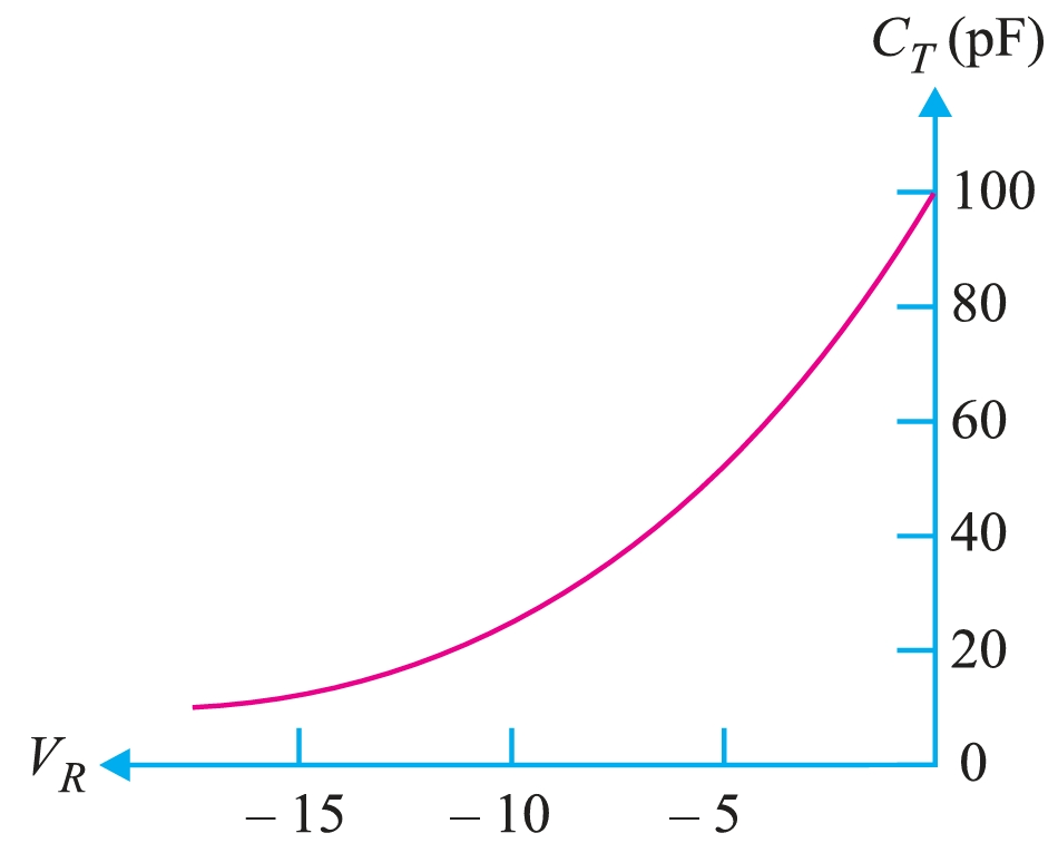
When reverse voltage across a varactor diode is increased, the width \(W_d\) of the depletion layer increases. Therefore, the total junction capacitance \(C_T\) of the junction decreases. On the other hand, if the reverse voltage across the diode is lowered, the width \(W_d\) of the depletion layer decreases. Consequently, the total junction capacitance \(C_T\) increases.
Fig. shows the curve between reverse bias voltage \(V_R\) across varactor diode and total junction capacitance \(C_T\). \(C_T\) can be changed simply by changing the voltage \(V_R\). For this reason, a varactor diode is sometimes called voltage-controlled capacitor.
Since the increase or decrease the junction capacitance of varactor diode simply by changing the reverse bias on the diode. This makes a varactor diode ideal for use in circuits that require voltage-controlled tuning.