Transistor
A transistor consists of two \(pn\)-junctions formed by sandwiching either \(p\)-type or \(n\)-type semiconductor between a pair of opposite types.
Accordingly, there are two types of transistors, namely:
- (i) \(n-p-n\) transistor
- (ii) \(p-n-p\) transistor
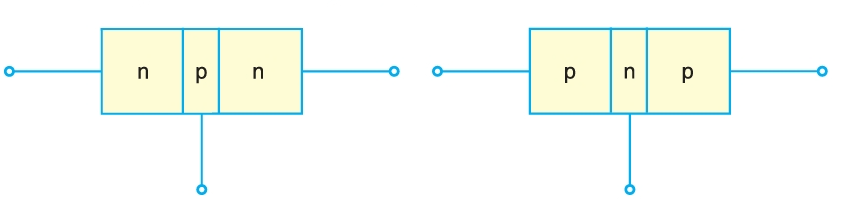
An \(n-p-n\) transistor is composed of two \(n\)-type semiconductors separated by a thin section of \(p\)-type as shown in Fig. 1 However, a \(p-n-p\) transistor is formed by two \(p\)-sections separated by a thin section of \(n\)-type as shown in Fig. 1.
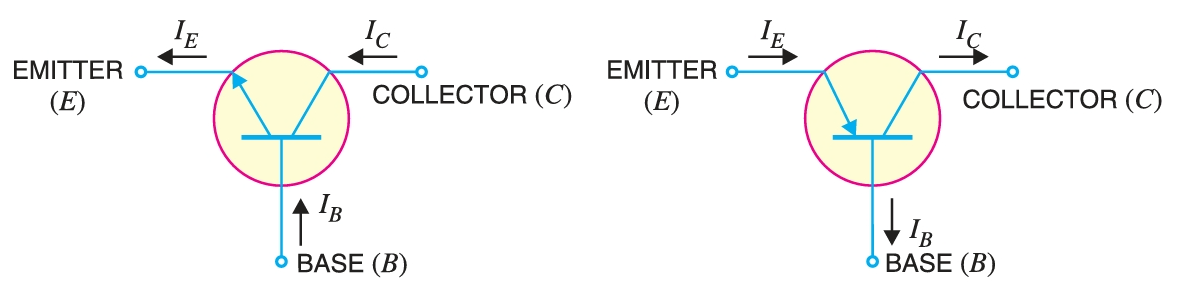
A transistor \(pnp\) or \(npn\) has three sections of doped semiconductors. The section on one side is the emitter and the section on the opposite side is the collector. The middle section is called the base and forms two junctions between the emitter and collector.
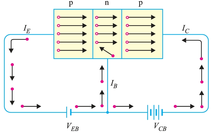
- (i) Emitter: The section on one side that supplies charge carriers (electrons or holes) is called the emitter. The emitter is always forward biased w.r.t. base so that it can supply a large number of majority carriers. In Fig. 2, the emitter \(p\)-type) of \(pnp\) transistor is forward biased and supplies hole charges to its junction with the base. Similarly, in Fig. 2, the emitter \(n\)-type) of \(npn\) transistor has a forward bias and supplies free electrons to its junction with the base.
- (ii) Collector: The section on the other side that collects the charges is called the collector. The collector is always reverse biased. Its function is to remove charges from its junction with the base. In Fig., the collector \(p\)-type) of \(pnp\) transistor has a reverse bias and receives hole charges that flow in the output circuit. Similarly, in Fig., the collector \(n\)-type) of \(npn\) transistor has reverse bias and receives electrons.
- (iii) Base: The middle section which forms two \(pn\)-junctions between the emitter and collector is called the base. The base-emitter junction is forward-biased, allowing low resistance for the emitter circuit. The base-collector junction is reverse-biased and provides high resistance in the collector circuit.
The transistor has two \(pn\) junctions, i.e., it is like two diodes. The junction between emitter and base may be called emitter-base diode or simply the emitter diode. The junction between the base and collector may be called collector-base diode or simply collector diode. The emitter diode is always forward biased whereas collector diode is always reverse biased.
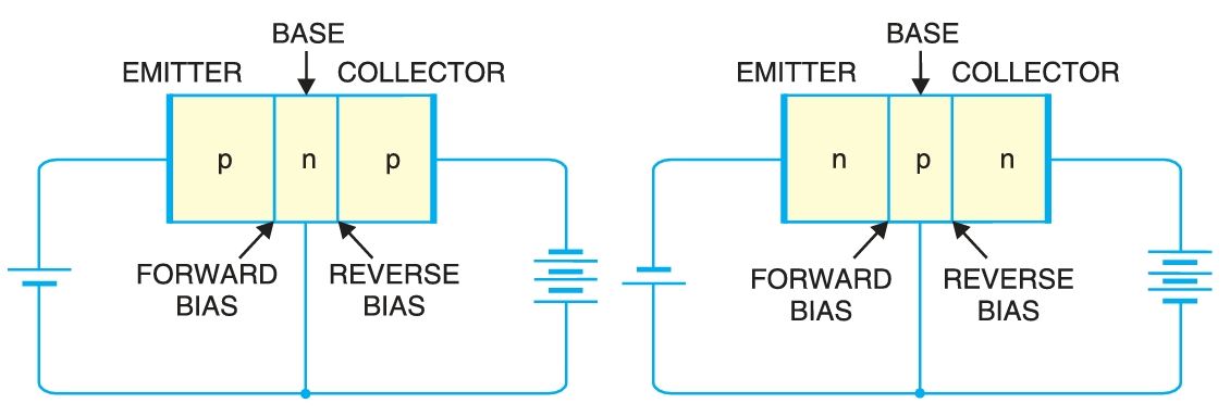
The emitter is heavily doped so that it can inject a large number of charge carriers (electrons or holes) into the base. The base is lightly doped and very thin; it passes most of the emitter injected charge carriers to the collector. The collector is moderately doped. The base is much thinner than the emitter, while the collector is wider than both. During transistor operation, much heat is produced at the collector junction. The collector is made larger to dissipate the heat. The resistance of the emitter diode (forward biased) is very small compared to the collector diode (reverse biased). Therefore, forward bias applied to the emitter diode is generally very small, whereas reverse bias on the collector diode is much higher.
Transistor Action
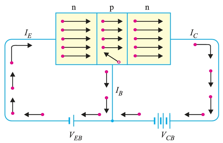
The emitter-base junction of a transistor is forward-biased, whereas the collector-base junction is reverse-biased. If, for a moment, we ignore the presence of the emitter-base junction, then practically no current would flow in the collector circuit because of the reverse bias. However, if the emitter-base junction is also present, then forward bias on it causes the emitter current to flow. It is observed that this emitter current flows almost entirely through the collector circuit. Therefore, the current in the collector circuit depends upon the emitter current. If the emitter current is zero, then the collector current is nearly zero. However, if the emitter current is \(1 ~mA\), then collector current is also about \(1 ~mA\). This is precisely what happens in a transistor. We shall now discuss this transistor action for \(npn\) and \(pnp\) transistors.
- (i) Working of \(npn\) transistor: Fig. shows the \(npn\) transistor with forward bias to emitter base junction and reverse bias to collector-base junction. The forward bias causes the electrons in the \(n\)-type emitter to flow towards the base. This constitutes the emitter current \(I_E\). As these electrons flow through the \(p\)-type base, they tend to combine with holes. As the base is lightly doped and very thin, therefore, only a few electrons (less than 5 %) combine with holes to constitute base current \(I_B\). The remainder (more than 95 %) cross over into the collector region to constitute collector current \(I_C\). In this way, almost the entire emitter current flows in the collector circuit. It is clear that emitter current is the sum of collector and base currents i.e. \[I_E = I_B + I_C\]
- (ii) Working of \(pnp\) transistor: Fig. shows the basic connection of a \(pnp\) transistor. The forward bias causes the holes in the \(p\)-type emitter to flow towards the base. This constitutes the emitter current \(I_E\). As these holes cross into \(n\)-type base, they tend to combine with the electrons. As the base is lightly doped and very thin, therefore, only a few holes (less than 5 %) combine with the electrons. The remainder (more than 95 %) cross into the collector region to constitute collector current \(I_C\). In this way, almost the entire emitter current flows in the collector circuit. The current conduction within the \(pnp\) transistor is by holes. However, in the external connecting wires, the current is still carried by electrons.
The input circuit (i.e., emitter-base junction) has low resistance because of forward bias, whereas the output circuit (i.e., collector-base junction) has high resistance due to reverse bias. The input emitter current flows almost entirely through the collector circuit. Therefore, a transistor transfers the input signal current from a low-resistance circuit to a high-resistance circuit. This is the key factor responsible for the amplifying capability of the transistor. The transistors are represented by schematic diagrams. The symbols used for \(npn\) and \(pnp\) transistors are shown in Fig.