Field Effect Transistors
A bipolar junction transistor (BJT) is a current-controlled device; i.e., its output characteristics are controlled by base current rather than base voltage. The ordinary or bipolar transistor has two principal disadvantages. First, it has a low input impedance because of the forward-biased emitter junction. Secondly, it has a considerable noise level. Although the low input impedance problem can be mitigated by careful design and the use of multiple transistors, it is difficult to achieve an input impedance above a few megohms. Meanwhile, the output characteristics are controlled by input voltage (i.e., electric field) and not by input current in a field effect transistor (FET). The field effect transistor (FET) has, by virtue of its construction and biasing, a large input impedance which may be more than \(100 \,\text{M}\Omega\). The FET is generally much less noisy than the ordinary or bipolar transistor. There are two basic types of field effect transistors, Junction field effect transistor (JFET) and Metal oxide semiconductor field effect transistor (MOSFET)
Junction Field Effect Transistor
A Junction Field Effect Transistor (JFET) is a three-terminal semiconductor device in which current conduction is by one type of carrier, i.e., electrons or holes.
The JFET was developed about the same time as the transistor, but it did not come into general use until the late 1960s. In a JFET, current conduction is either by electrons or by holes, and is controlled by an electric field between the gate electrode and the device's conducting channel. The JFET has high input impedance and low noise level.
Construction
A JFET consists of a \(p-\)type or \(n-\)type silicon bar containing two pn junctions at the sides, as shown in Fig. 1. The bar forms the conducting channel for the charge carriers. If the bar is of \(n-\)type, it is called \(n-\)channel JFET as shown in Fig. 1, and if the bar is of \(p-\)type, it is called a \(p-\)channel JFET as shown in Fig. 1. The two \(pn\)-junctions forming diodes are connected internally, and a common terminal called \(\text{Gate}\) is taken out. Other terminals are \(\text{Source}\) and \(\text{Drain}\) taken out from the bar as shown. Thus a JFET has essentially three terminals viz., gate \((G)\), source \((S)\) and drain \((D)\).
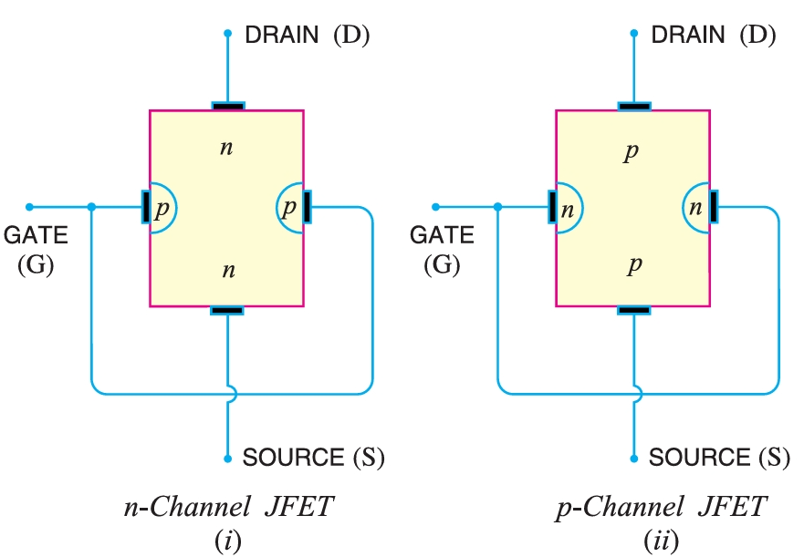
Fig. 2(i) shows \(n-\)channel JFET polarities whereas Fig. 2(ii) shows the \(p-\)channel JFET polarities. Note that in each case, the gate-source voltage is such that the gate is reverse-biased. This is the normal way to connect a JFET. The drain and source terminals are interchangeable; either end can be used as a source, and the other as a drain.
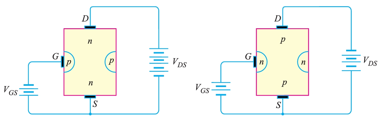
The input circuit (i.e., gate-to-source) of a JFET is reverse-biased. This means that the device has high input impedance. The drain is so biased with respect to the source that the drain current \(I_{\text{D}}\) flows from the source to the drain. In all JFETs, source current \(I_{S}\) is equal to the drain current i.e.
\[ I_{S} = I_{\text{D}}\]
Principle
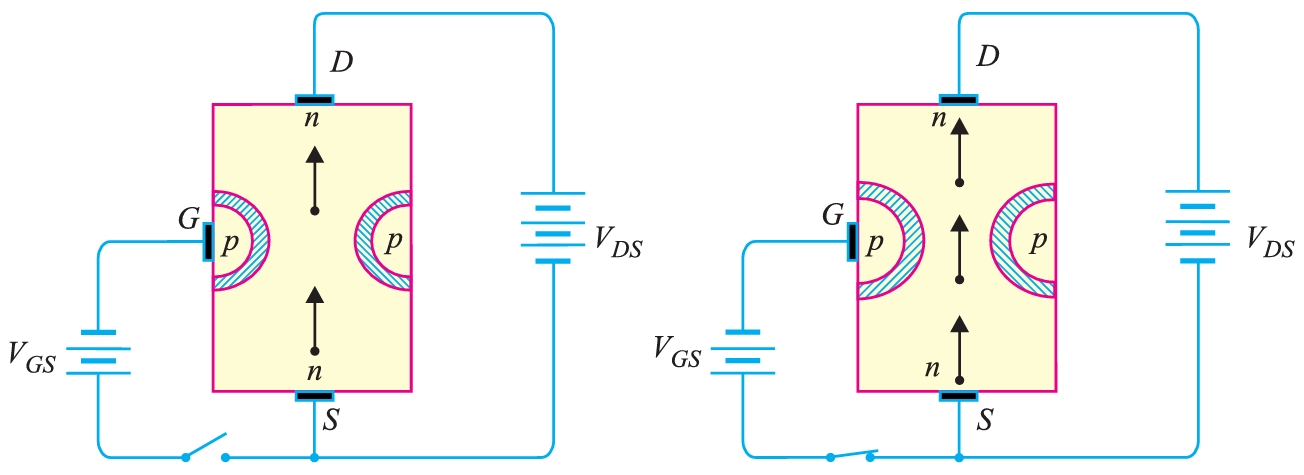
Fig. 3 shows the circuit of an \(n-\)channel JFET with normal polarities. Note that the gate is reverse-biased. The two \(pn\)-junctions at the sides form two depletion layers. The current is carried by charge carriers (i.e., free electrons in this case) through the channel between the two depletion layers and out of the drain. The width and hence resistance of this channel can be controlled by changing the input voltage \(V_{\text{GS}}\). The greater the reverse voltage \(V_{\text{GS}}\), the wider the depletion layers will be and the narrower the conducting channel. The narrower channel means greater resistance, and hence the source-to-drain current decreases. Reverse will happen should \(V_{\text{GS}}\) decrease. Thus, JFET operates on the principle that the width and hence the resistance of the conducting channel can be varied by changing the reverse voltage \(V_{\text{GS}}\). In other words, the magnitude of drain current \((I_{\text{D}})\) can be changed by altering \(V_{\text{GS}}\).
Working
When a voltage \(V_{\text{DS}}\) is applied between drain and source terminals and the voltage on the gate is zero [ See Fig. 3 (i) ], the two \(pn\)-junctions at the sides of the bar establish depletion layers. The electrons will flow from source to drain through a channel between the depletion layers. The thickness of these layers determines the channel width and, hence, the current conduction through the bar.
When a reverse voltage \(V_{\text{GS}}\) is applied between the gate and source [See Fig. 3 (ii)], the width of the depletion layers is increased. This reduces the width of the conducting channel, thereby increasing the resistance of the \(n-\)type bar. Consequently, the current from source to drain is decreased. On the other hand, decreasing the reverse gate voltage decreases the width of the depletion layers. This increases the width of the conducting channel and hence the source-to-drain current.
It is clear from the above discussion that the current from source to drain can be controlled by applying a potential (i.e., an electric field) to the gate. For this reason, the device is called a field effect transistor. It may be noted that a \(p-\)channel JFET operates in the same manner as an \(n-\)channel JFET except that channel current carriers will be the holes instead of electrons and the polarities of \(V_{\text{GS}}\) and \(V_{\text{DS}}\) are reversed.
When the reverse voltage \(V_{\text{GS}}\) on the gate is continuously increased, a state is reached when the two depletion layers touch each other, and the channel is cut off. Under such conditions, the channel becomes a non-conductor.
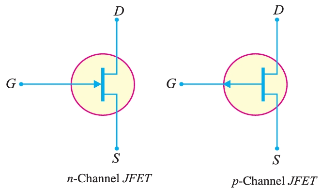
Fig. 4 shows the schematic symbol of a JFET. The vertical line in the symbol may be thought of as a channel and source \((S)\) and drain \((D)\) connected to this line. If the channel is \(n-\)type, the arrow on the gate points towards the channel as shown in Fig. 4 (i). However, for the \(p-\)type channel, the arrow on the gate points from channel to gate. A JFET acts like a voltage-controlled device, i.e., input voltage (\(V_{\text{GS}}\)) controls the output current. This is different from ordinary transistor (or bipolar transistor) where input current controls the output current. Thus, a JFET is a semiconductor device that acts like a vacuum tube. The need for JFETs arose because, as modern electronic equipment became increasingly transistorised, it became apparent that many functions in which bipolar transistors could not replace vacuum tubes. Owing to their extremely high input impedance, JFET devices are more like vacuum tubes than bipolar transistors and can therefore take over many vacuum-tube functions. Thus, because of JFETs, electronic equipment is closer today to being completely solid-state.
JFET devices have not only taken over the functions of vacuum tubes but are now also threatening to depose bipolar transistors as the most widely used semiconductor devices. As an amplifier, the JFET has higher input impedance than a conventional transistor, generates less noise, and is more radiation-resistant.
Fig. 5 shows JFET amplifier circuit. The weak signal is applied between gate and source and amplified output is obtained in the drain-source circuit.
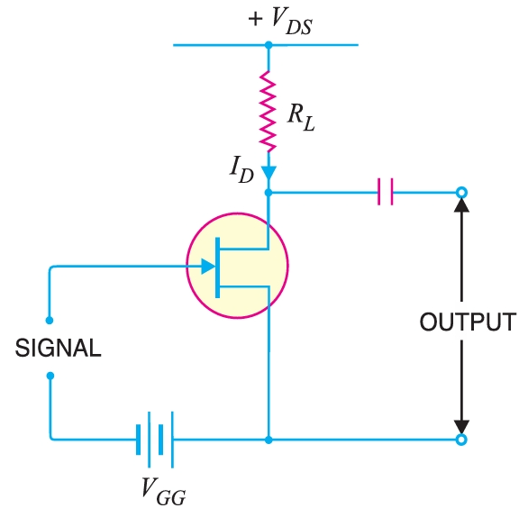
For the proper operation of JFET, the gate must be negative w.r.t. source i.e., input circuit should always be reverse biased. This is achieved either by inserting a battery \(V_{\text{GG}}\) in the gate circuit or by a circuit known as biasing circuit. In the present case, we are providing biasing by the battery \(V_{\text{GG}}\).
A small change in the reverse bias on the gate produces a large change in drain current. This fact makes JFET capable of raising the strength of a weak signal. During the positive half of signal, the reverse bias on the gate decreases. This increases the channel width and hence the drain current. During the negative half-cycle of the signal, the reverse voltage on the gate increases. Consequently, the drain current decreases. The result is that a small change in voltage at the gate produces a large change in drain current. These large variations in drain current produce large output across the load \(RL\). In this way, JFET acts as an amplifier.
Output Characteristics
The curve between drain current \((I_{\text{D}})\) and drain-source voltage (\(V_{\text{DS}}\) ) of a JFET at constant gate source voltage (\(V_{\text{GS}}\)) is known as output characteristics of JFET. Fig. 6(i) shows the circuit for determining the output characteristics of a JFET. Keeping \(V_{\text{GS}}\) fixed at a given value, the drain-source voltage is varied in steps. Corresponding to each value of \(V_{\text{DS}}\), the drain current \(I_{\text{D}}\) is noted. A plot of these values gives the output characteristic of JFET at \(V_{\text{GS}}\). By repeating a similar procedure, output characteristics at other gate-source voltages can be plotted. Fig. 6(ii) shows a family of output characteristics.
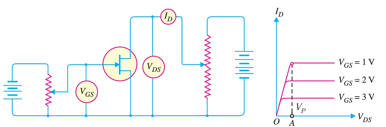
At first, the drain current \(I_{\text{D}}\) rises rapidly with drain-source voltage \(V_{\text{DS}}\) but then becomes constant. The drain-source voltage above which the drain current becomes constant is known as the pinch-off voltage. Thus, in Fig. 6(ii), \(OA\) is the pinch off voltage \(V_{\text{P}}\).
After the pinch-off voltage, the channel width becomes so narrow that the depletion layers nearly touch. The drain current passes through the small passage between these layers. Therefore, the increase in drain current is very small with \(V_{\text{DS}}\) above the pinch off voltage. Consequently, drain current remains constant.
Features
The salient features of JFET are :
- A JFET is a three-terminal voltage-controlled semiconductor device, i.e., input voltage controls the output characteristics of the JFET.
- The JFET is always operated with the gate-source pn junction reverse-biased.
- In a JFET, the gate current is zero, i.e., \(I_{G} = 0\,\text{A}\).
- Since there is no gate current, \(I_{\text{D}} = I_{S}\).
- The JFET must be operated between \(V_{\text{GS}}\) and \(V_{\text{GS(off)}}\) . For this range of gate-to-source voltages, \(I_{\text{D}}\) will range from \(I_{\text{DSS}}\) to almost zero.
- Because the two gates are at the same potential, both depletion layers widen or narrow down by an equal amount.
- The JFET is not subjected to thermal runaway when the temperature of the device increases.
- The drain current \(I_{\text{D}}\) is controlled by changing the channel width.
- Since JFET has no gate current, there is no \(\beta\) rating of the device.
Shorted-gate drain current
It is the drain current with source short-circuited to gate (i.e. \(V_{\text{GS}}\) = 0) and drain voltage (\(V_{\text{DS}}\)) equal to pinch off voltage.
It is sometimes called zero-bias current. Fig. 7 shows the JFET circuit with \(V_{\text{GS}}= 0\) , i.e., source shorted-circuited to gate. This is normally called the shorted-gate condition. Fig. 7 shows the graph between \(I_{\text{D}}\) and \(V_{\text{DS}}\) for the shorted gate condition. The drain current rises rapidly at first, then levels off at the pinch-off voltage \(V_{\text{P}}\). The drain current has now reached the maximum value \(I_{\text{DSS}}\). When \(V_{\text{DS}}\) is increased beyond \(V_{\text{P}}\), the depletion layers expand at the top of the channel. The channel now acts as a current limiter, holding the drain current constant at \(I_{\text{DSS}}\).
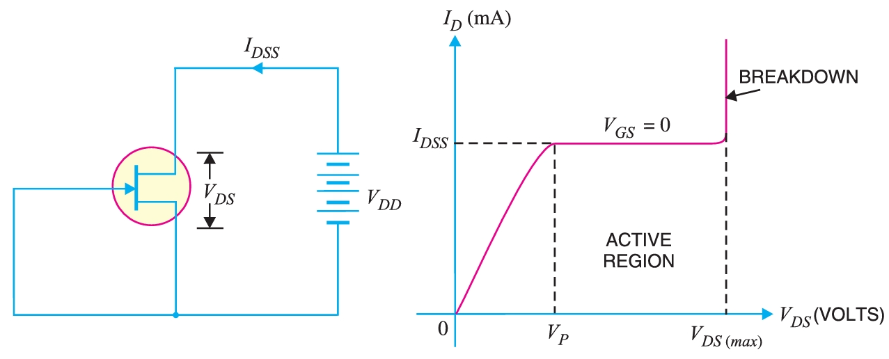
Since \(I_{\text{DSS}}\) is measured under shorted-gate conditions, it is the maximum drain current achievable in normal JFET operation. There is a maximum drain voltage [\(V_{\text{DS}}\) (max)] that can be applied to a JFET. If the drain voltage exceeds \(V_{DS(\text{max})}\) , the JFET would break down as shown in Fig. 7. The region between \(V_{\text{P}}\) and \(V_{DS(\text{max})}\) (breakdown voltage) is called the constant-current region or active region. As long as \(V_{\text{DS}}\) is kept within this range, \(I_{\text{D}}\) will remain constant for a constant value of \(V_{\text{GS}}\). In other words, in the active region, the JFET behaves as a constant–current device. For proper working of the JFET, it must be operated in the active region.
Pinch off Voltage
It is the minimum drain-source voltage at which the drain current essentially becomes constant.
Figure 8 shows the drain curves of a JFET. Note that pinch off voltage is \(V_{\text{P}}\). The highest curve is for \(V_{\text{GS}}= 0\,\text{V}\) , the shorted-gate condition. For values of \(V_{\text{DS}}\) greater than \(V_{\text{P}}\), the drain current is almost constant. It is because when \(V_{\text{DS}}\) equals \(V_{\text{P}}\), the channel is effectively closed and does not allow further increase in drain current. It may be noted that for the proper function of a JFET, it is always operated for \(V_{\text{DS}}\) > \(V_{\text{P}}\). However, \(V_{\text{DS}}\) should not exceed \(V_{DS(\text{max})}\) otherwise JFET may breakdown.
Gate-source cut-off voltage.
It is the gate-source voltage where the channel is completely cut off and the drain current becomes zero.
The idea of gate-source cut-off voltage can be easily understood if we refer to the transfer characteristic of a JFET shown in Fig. 8. As the reverse gate-source voltage is increased, the cross-sectional area of the channel decreases. This, in turn, decreases the drain current. At some reverse gate-source voltage, the depletion layers extend completely across the channel. In this condition, the channel is cut off, and the drain current reduces to zero. The gate voltage at which the channel is cut off (i.e., channel becomes non-conducting) is called gate-source cut off voltage \(V_{\text{GS(off)}}\) .
It is interesting to note that \(V_{\text{GS(off)}}\) will always have the same magnitude value as \(V_{\text{P}}\). There is a distinct difference between \(V_{\text{P}}\) and \(V_{\text{GS(off)}}\). The \(V_{\text{P}}\) is the value of \(V_{\text{DS}}\) that causes the JEFT to become a constant current device. It is measured at \(V_{\text{GS}}= 0 \,\text{V}\) and will have a constant drain current = \(I_{\text{DSS}}\). However, \(V_{\text{GS(off)}}\) is the value of \(V_{\text{GS}}\) that causes \(I_{\text{D}}\) to drop to nearly zero.
The relation between \(I_{\text{DSS}}\) and \(V_{\text{P}}\) is shown in Fig. 8. We note that gate-source cut off voltage [i.e., \(V_{\text{GS(off)}}\)] on the transfer characteristic is equal to pinch off voltage \(V_{\text{P}}\) on the drain characteristic, i.e.,
\[V_{\text{P}} = | V_{\text{GS(off)}}| \]
For example, if a JFET has \(V_{GS(\text{off}) = − 4\,\text{V}}\), then \(V_{\text{P}}= 4\,\text{V}\). The transfer characteristic of the JFET shown in Fig. 8 is part of a parabola. A rather complex mathematical analysis yields the following expression for drain current :
\[\boxed{I_{\text{D}} = I_{\text{DSS}}\left( 1 − \frac{V_{\text{GS}}}{V_{\text{GS(off)}}}\right)^{2}}\]
where, \(I_{\text{D}}\) is drain current at given \(V_{\text{GS}}\), \(I_{\text{DSS}}\) is shorted – gate drain current, \(V_{\text{GS}}\) is the gate–source voltage, \(V_{\text{GS(off)}}\) is gate–source cut-off voltage.
Advantages
A JFET is a voltage-controlled, constant current device in which variations in input voltage control the output current.
The advantages of a JFET are :
- It has a very high input impedance (of the order of \(100 \,\text{M}\Omega\)). This permits a high degree of isolation between the input and output circuits.
- The operation of a JFET depends upon the bulk material current carriers that do not cross junctions. Therefore, the inherent noise of tubes (due to high-temperature operation) and that of transistors (due to junction transitions) are not present in a JFET.
- A JFET has a negative temperature coefficient of resistance. This avoids the risk of thermal runaway.
- A JFET has a very high power gain. This eliminates the need for driver stages.
- A JFET has a smaller size, longer life, and high efficiency.
JFET parameters
A JFET has certain parameters that determine its performance in a circuit. The main parameters of a JFET are (i) a.c. drain resistance (ii), transconductance (iii), and amplification factor.
a.c. drain resistance.
Corresponding to the a.c. plate resistance, we have a.c. drain resistance \((r_{d})\) in a JFET.
It is the ratio of change in drain-source voltage \((\Delta V_{\text{DS}})\) to the change in drain current \((\Delta I_{\text{D}})\) at constant gate-source voltage
i.e., a.c. drain resistance, \(r_{d}\),
\[\boxed{r_{d}= \frac{\Delta V_{\text{DS}}}{\Delta I_{\text{D}}} \bigg|_{\text{at constant}\, V_{\text{GS}}}}\]
The change in \(I_{\text{D}}\) is small for a change in \(V_{\text{DS}}\) because the curve is almost flat above the pinch off voltage. Therefore, the drain resistance of a JFET has a large value, ranging from \(10 \,\text{k}\,\Omega\) to \(1 \,\text{M}\,\Omega\).
Transconductance
The control that the gate voltage has over the drain current is measured by transconductance \((g_{\text{fs}})\).
It is the ratio of change in drain current \((\Delta I_{\text{D}})\) to the change in gate-source voltage \(\Delta V_{(\text{GS}})\) at constant drain-source voltage, i.e., Transconductance, \(g_{\text{fs}}\)
\[\boxed{g_{\text{fs}}= \frac{\Delta I_{\text{D}}}{\Delta V_{\text{GS}}} \bigg|_{\text{at constant}\, V_{\text{DS}}}}\]
The transconductance of a JFET is usually expressed in mA/V or µS.
Amplification factor
It is the ratio of change in drain-source voltage \((\Delta V_{\text{DS}})\) to the change in gate-source voltage \((\Delta V_{\text{GS}})\) at constant drain current, i.e., Amplification factor, \(\mu\)
\[\boxed{\mu = \frac{\Delta V_{\text{DS}}}{\Delta V_{\text{GS}}} \bigg|_{\text{at constant}\, I_{\text{D}}}}\]
Amplification factor of a JFET indicates how much more control the gate voltage has over drain current than has the drain voltage. For instance, if the amplification factor of a JFET is \(50\), it means that the gate voltage is \(50\) times as effective as the drain voltage in controlling the drain current.
Relation of JFET Parameters
The relationship among JFET parameters can be established as:
\[\mu = \frac{\Delta V_{\text{DS}}}{\Delta V_{\text{GS}}}\]
Multiplying the numerator and denominator on R.H.S. by \(\Delta I_{\text{D}}\), we get,
\[\mu = \frac{\Delta V_{\text{DS}}}{\Delta V_{\text{GS}}} \times \frac{\Delta I_{\text{D}}}{\Delta I_{\text{D}}} \]
\[\mu = \frac{\Delta V_{\text{DS}}}{\Delta I_{\text{D}}} \times \frac{\Delta I_{\text{D}}}{\Delta V_{\text{GS}}}\]
\[\therefore \quad \boxed {\mu = r_{d} \times g_{\text{fs}}}\]
\[\therefore \quad \text{i.e., amplification factor = a.c. drain resistance} \times \,\text{transconductance}\]
Variation of Transconductance
The transconductance \(g_{\text{m}}\) of a JFET is the ratio of a change in drain current \((\Delta I_{\text{D}})\) to a change in gate-source voltage \((\Delta V_{\text{GS}})\) at constant \(V_{\text{DS}}\), i.e.
\[\boxed{g_{\text{m}} = {\Delta I_{\text{D}}}{\Delta V_{\text{GS}}}} \]
The transconductance \(g_{\text{m}}\) of a JFET is an important parameter because it is a major factor in determining the voltage gain of JFET amplifiers. However, the transfer characteristic curve for a JFET is non-linear so that the value of \(g_{\text{m}}\) depends upon the location on the curve. Thus, the value of \(g_{\text{m}}\) at point \(A\) in Fig. 8 will be different from that at point \(B\). The equation to determine the value of \(g_{\text{m}}\) at a specified value of \(V_{\text{GS}}\) :
\[ \boxed{g_{\text{m}}= g_{\text{mo}} \left(1-\frac{V_{\text{GS}}}{V_{\text{GS(off)}}}\right)}\]
where \(g_{\text{m}}\) is the value of transconductance at any point on the transfer characteristic curve, \(g_{\text{mo}}\) is the value of transconductance (maximum) at \(V_{\text{GS}}= 0\).
Normally, the data sheet provides the \(g_{\text{mo}}\) value. When the value of \(g_{\text{mo}}\) is not available, it is approximately calculate \(g_{\text{mo}}\) using the following relation :
\[g_{\text{mo}} = \frac{2\,I_{\text{DSS}}}{|V_{\text{GS(off)}}|} \]