Metal Oxide Semiconductor FET
A JFET can only be operated in the depletion mode. The main drawback of JFET is that its gate must be reverse-biased for proper operation of the device, i.e., it can only have negative gate operation for \(n-\)channel and positive gate operation for \(p-\)channel. This means that we can only decrease the width of the channel (i.e., decrease the conductivity of the channel) from its zero-bias size. This type of operation is called depletion-mode operation in which the JFET operates. However, there is a field effect transistor (FET) that can be operated to enhance (or increase) the width of the channel (with consequent increase in conductivity of the channel), i.e., it can have enhancement-mode operation. Such an FET is called a MOSFET.
A field effect transistor (FET) that can be operated in the enhancement-mode is called a MOSFET.
A MOSFET is an important semiconductor device and can be used in any of the circuits covered for JFET. However, a MOSFET has several advantages over a JFET, including high input impedance and lower production cost. There are two basic types of MOSFETs, viz. (a) Depletion-type MOSFET or D-MOSFET and (b) Enhancement-type MOSFET or E-MOSFET.
The D-MOSFET can be operated in both depletion and enhancement modes. For this reason, a D-MOSFET is sometimes called the depletion/enhancement MOSFET. The E-MOSFET can be operated only in enhancement mode. The manner in which a MOSFET is constructed determines whether it is a D-MOSFET or an E-MOSFET.
D-MOSFET
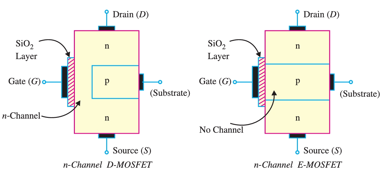
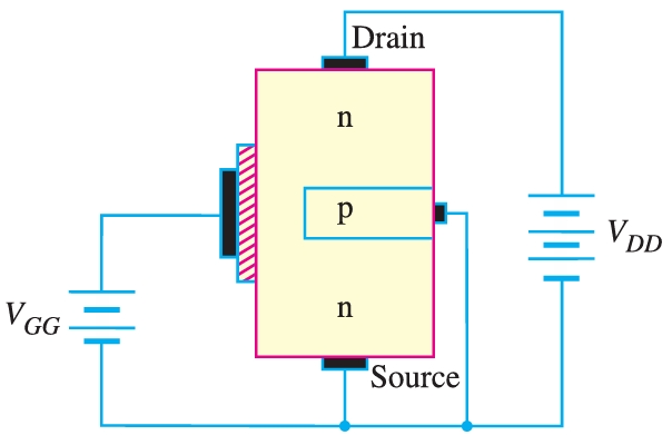
Fig. 2 shows the constructional details of the \(n-\)channel D-MOSFET. It is similar to an \(n-\)channel JFET except with the few changes. The \(n-\)channel D-MOSFET is a piece of \(n-\)type material with a \(p-\)type region (called substrate) on the right and an insulated gate on the left, as shown in Fig. 2.
The free electrons in the \(n-\)channel flowing from source to drain must pass through the narrow channel between the gate and the \(p-\)type region (i.e., substrate). A thin layer of metal oxide (usually silicon dioxide, SiO\(_{2}\)) is deposited over a small portion of the channel. A metallic gate is deposited over the oxide layer. As SiO\(_{2}\) is an insulator, the gate is insulated from the channel. Note that the arrangement forms a capacitor. One plate of this capacitor is the gate, and the other plate is the channel with SiO\(_{2}\) as the dielectric. The substrate is connected to the source (S) internally so that a MOSFET has three terminals, viz., source (S), gate (G), and drain (D). Since the gate is insulated from the channel, we can apply either a negative or a positive voltage to the gate. Therefore, D-MOSFET can be operated in both depletion-mode and enhancement-mode. However, a JFET can be operated only in depletion mode.
There are two types of D-MOSFETs, i.e., \(n-\)channel and \(p-\)channel D-MOSFET.
n-channel D-MOSFET
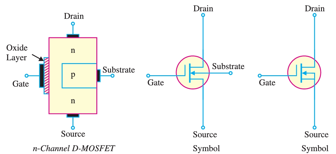
Fig. 2 (i) shows the various parts of an \(n-\)channel D-MOSFET. The \(p-\)type substrate narrows the channel between the source and drain, leaving only a small passage on the left. Electrons flowing from the source (when the drain is positive with respect to the source) must pass through this narrow channel. The symbol for \(n-\)channel D-MOSFET is shown in Fig. 2 (ii). The gate appears like a capacitor plate. Just to the right of the gate is a thick vertical line representing the channel. The drain lead exits the top of the channel, and the source lead connects to the bottom. The arrow is on the substrate and points to the n-material; therefore, we have an \(n-\)channel D-MOSFET. It is a usual practice to connect the substrate to the source internally, as shown in Fig. 2 (iii). This results in a three-terminal device.
p-channel D-MOSFET
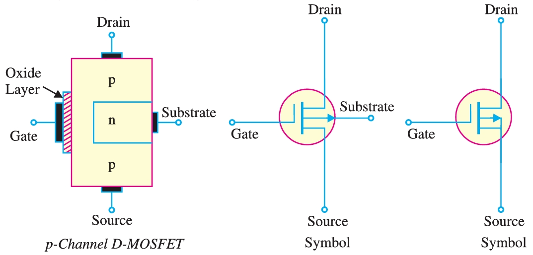
Fig. 3 (i) shows the various parts of the \(p-\)channel D-MOSFET. The \(n-\)type substrate narrows the channel between the source and drain, leaving only a small passage on the left. Conduction occurs through the flow of holes from the source to the drain through this narrow channel. The symbol for \(p-\)channel D-MOSFET is shown in Fig. 3 (ii). It is a usual practice to connect the substrate to the source internally. This results in a three-terminal device whose schematic symbol is shown in Fig. 3 (iii).
Circuit Operation
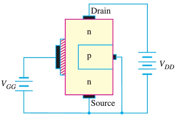
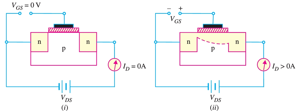
Fig. 4 (i) shows the circuit of an \(n-\)channel D-MOSFET. The gate forms a small capacitor. One plate of this capacitor is the gate, and the other is the channel, with a metal oxide dielectric. When the gate voltage changes, the capacitor's electric field changes, which in turn changes the resistance of \(n-\)channel. Since the gate is insulated from the channel, either a negative or a positive voltage is applied to the gate. The negative-gate operation is called depletion mode, whereas the positive-gate operation is known as enhancement mode.
Depletion mode.
Fig. 4 (i) shows depletion-mode operation of an \(n-\)channel D-MOSFET. Since the gate is negative, it means electrons are on the gate as shown in Fig. 4 (ii). These electrons repel the free electrons in the \(n-\)channel, leaving a layer of positive ions in a part of the channel as shown in Fig. 4 (ii). In other words, the \(n-\)channel is depleted (i.e., emptied) of some of its free electrons. Therefore, fewer free electrons are available for current conduction in the \(n-\)channel. This is equivalent to increasing the resistance of the channel. The greater the negative gate voltage, the lower the current from source to drain. Thus, the \(n-\)channel resistance can be controlled by varying the negative gate voltage and, hence, the current from source to drain. The action of the D-MOSFET is similar to that of a JFET with a negative voltage to the gate. Because the action with the negative gate depends upon depleting (i.e., emptying) the channel of free electrons, the negative-gate operation is called depletion mode.
Enhancement mode.
Fig. 5 (i) shows the enhancement-mode operation of an \(n-\)channel D MOSFET. Again, the gate acts like a capacitor. Since the gate is positive, it induces negative charges in the \(n-\)channel as shown in Fig. 5 (ii). These negative charges are the free electrons drawn into the channel. Because these free electrons are added to those already in the channel, the total number of free electrons in the channel is increased. Thus, a positive gate voltage increases the conductivity of the channel. The greater the positive gate voltage, the greater the conduction from source to drain.
Thus, applying a positive voltage to the gate allows to control the conductivity of the channel. The main difference between a D-MOSFET and a JFET is that we can apply a positive gate voltage to a D-MOSFET and still have essentially zero current. Because the action with a positive gate depends upon enhancing the conductivity of the channel, the positive gate operation is called enhancement mode.
In a D-MOSFET, the source to drain current is controlled by the electric field of the capacitor formed at the gate. The gate of a JFET behaves as a reverse-biased diode, whereas the gate of a D-MOSFET acts like a capacitor. For this reason, a D-MOSFET can be operated with either a positive or a negative gate voltage. As the gate of D-MOSFET forms a capacitor, therefore, negligible gate current flows whether positive or negative voltage is applied to the gate. For this reason, the input impedance of D-MOSFET is very high, ranging from \(10,000 \,\text{M}\Omega\) to \(10,000,00 \,\text{M}\Omega\). The extremely small dimensions of the oxide layer under the gate terminal result in a very low capacitance, and the D-MOSFET has, therefore, a very low input capacitance. This characteristic makes the D-MOSFET useful in high-frequency applications.
Transfer Characteristics
Fig. 6 shows the transfer characteristic (or transconductance) curve for an \(n-\)channel D-MOSFET. The point on the curve where \(V_{\text{GS}}= 0\) , \(I_{\text{D}} = I_{\text{DSS}}\). It is expected because \(I_{\text{DSS}}\) is the value of \(I_{\text{D}}\) when gate and source terminals are shorted, i.e., \(V_{\text{GS}}= 0\) .
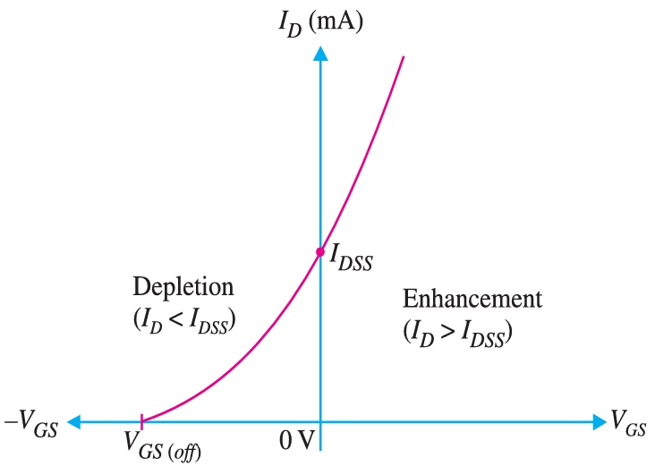
As \(V_{\text{GS}}\) goes negative, \(I_{\text{D}}\) decreases below the \(I_{\text{DSS}}\) value until \(I_{\text{D}}\) reaches zero at \(V_{\text{GS}}\) = \(V_{GS(\text{off})}\) , just as with a JFET. When \(V_{\text{GS}}\) is positive, \(I_{\text{D}}\) exceeds \(I_{\text{DSS}}\). The maximum allowable \(I_{\text{D}}\) value is specified in the data sheet for the D-MOSFET. The transconductance curve for the D-MOSFET is very similar to the curve for a JFET. Because of this similarity, the JFET and the DMOSFET have the same transconductance equation, viz.
\[I_{\text{D}} = I_{\text{DSS}} \left(1 − \frac{V_{\text{GS}}}{V_{\text{GS(off)}}} \right)^{2}\]
Transconductance
The value of gm is found for a D-MOSFET in the same way that it is for the JFET, i.e.
\[g_{\text{m}} = g_{\text{mo}} \left(1-\frac{V_{\text{GS}}}{V_{\text{GS(off)}}} \right)\]
Input Impedance
The gate impedance of a D-MOSFET is extremely high. For example, a typical D-MOSFET may have a maximum gate current of \(10 \,\text{pA}\) when \(V_{\text{GS}}= 35 \,\text{V}\) . Therefore, input impedance, \(Z_{i}\),
\[Z_{i} = \frac{35\,\text{V}}{10\,\text{pA}} = \frac{35\,\text{V}}{10\times10^{-12}\,\text{A}} = 3.5 \times 10^{12}\Omega \]
With an input impedance in this range, the D-MOSFET would present virtually no load to a source circuit.
D-MOSFETs vs. JFETs
| Device | JFET | D-MOSFET |
|---|---|---|
| Modes of operation: | Depletion only | Depletion and enhancement |
| Bias circuits: | Gate bias, Self bias, Voltage-divider bias |
Gate bias, Self bias, Voltage-divider bias, Zero bias |
| Advantages: | Extremely high input impedance | Higher input impedance than a JFET. Can operate in both modes (depletion and enhancement). |
| Disadvantages: | Bias instability. It can operate only in the depletion mode. |
Bias instability. Sensitive to changes in temperature than a JFET. |
E-MOSFET
Fig. 7 shows the constructional details of the \(n-\)channel E-MOSFET. Its gate construction is similar to that of D-MOSFET. The E-MOSFET has no channel between source and drain, unlike the D-MOSFET. Note that the substrate extends to the SiO\(_{2}\) layer, so there is no channel. The E-MOSFET requires a proper gate voltage to form a channel (called an induced channel). The E-MOSFET can be operated only in enhancement mode. In short, the construction of E-MOSFET is quite similar to that of the D-MOSFET except for the absence of a channel between the drain and source terminals.
Circuit Operation
First, E-MOSFET operates only in the enhancement mode and has no depletion mode. Secondly, the E-MOSFET has no physical channel from source to drain because the substrate extends to the SiO\(_{2}\) layer [See Fig. 8(i)]. It is only by applying a \(V_{\text{GS}}\) (gate-to-source voltage) of the proper magnitude and polarity that the device begins to conduct. The minimum value of \(V_{\text{GS}}\) of proper polarity that turns on the E-MOSFET is called Threshold voltage [\(V_{\text{GS(th)}}\) ]. The \(n-\)channel device requires positive \(V_{\text{GS}} (\geq V_{\text{GS(th)}})\) and the \(p-\)channel device requires negative \(V_{\text{GS}} (\leq V_{\text{GS(th)}})\).
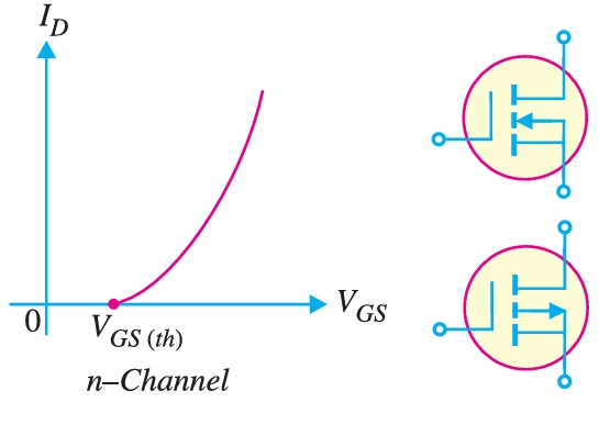
Fig. 8 (i) shows the circuit of an \(n-\)channel E-MOSFET. When \(V_{\text{GS}}= 0\,\text{V}\) [See Fig. 8(i)], there is no channel connecting the source and drain. The \(p\)-substrate has only a few thermally produced free electrons (minority carriers), so that the drain current is essentially zero. For this reason, E-MOSFET is normally \(OFF\) when \(V_{\text{GS}}= 0 \,\text{V}\). This behaviour of E-MOSFET is quite different from JFET or D-MOSFET.
When the gate is made positive (i.e., \(V_{\text{GS}}\) is positive), as shown in Fig. 8 (ii), it attracts free electrons into the \(p\)-region. The free electrons combine with the holes next to the SiO\(_{2}\) layer. If \(V_{\text{GS}}\) is sufficiently positive, all the holes at the SiO\(_{2}\) interface are filled, and free electrons begin to flow from the source to the drain. The effect is the same as creating a thin layer of \(n-\)type material (i.e., inducing a thin \(n-\)channel) adjacent to the SiO\(_{2}\) layer. Thus, the E-MOSFET is turned \(ON\), and the drain current \(I_{\text{D}}\) starts flowing from the source to the drain. The minimum \(V_{\text{GS}}\) required to turn the E-MOSFET \(ON\) is called the threshold voltage [\(V_{\text{GS(th)}}\)].
When \(V_{\text{GS}}\) is less than \(V_{\text{GS(th)}}\), there is no induced channel, and the drain current \(I_{\text{D}}\) is zero. When \(V_{\text{GS}}\) is equal to \(V_{\text{GS(th)}}\), the E-MOSFET is turned \(ON\), and the induced channel conducts drain current from the source to the drain. Beyond \(V_{\text{GS(th)}}\), if the value of \(V_{\text{GS}}\) is increased, the newly formed channel becomes wider, causing \(I_{\text{D}}\) to increase. If the \(V_{\text{GS}}\) voltage decreases [not less than \(V_{\text{GS(th)}}\)], the channel narrows and \(I_{\text{D}}\) decreases. This fact is revealed by the transconductance curve of \(n-\)channel E-MOSFET shown in Fig. 8. As you can see, \(I_{\text{D}} = 0\) when \(V_{\text{GS}}= 0\). Therefore, the \(I_{\text{DSS}}\) of the E-MOSFET is zero. Note also that there is no drain current until \(V_{\text{GS}}\) reaches \(V_{\text{GS(th)}}\).
Fig. 8 (i) shows the schematic symbols for an \(n-\)channel E-MOSFET, whereas Fig. 8 (ii) shows the schematic symbol for a \(p-\)channel E-MOSFET. When \(V_{\text{GS}}= 0\) , the E-MOSFET is \(OFF\) because there is no conducting channel between the source and drain. The broken channel line in the symbols indicates the normally \(OFF\) condition.
Transconductance Relation
Fig. 9 shows the transconductance curve for an \(n-\)channel E-MOSFET. This curve is different from the transconductance curve for an \(n-\)channel JFET or an \(n-\)channel D-MOSFET. It is because it starts at \(V_{\text{GS(th)}}\) rather than \(V_{\text{GS(off)}}\) on the horizontal axis and never intersects the vertical axis. The equation for the E-MOSFET transconductance curve (for \(V_{\text{GS}} \gt V_{\text{GS(th)}}\)) is
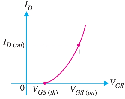
\[I_{\text{D}} = K (V_{\text{GS}} – V_{\text{GS(th)}} )^{2}\]
The constant \(K\) depends on the particular E-MOSFET, and its value is determined from the following equation :
\[K= \frac{I_{D\text{(on)}}}{(V_{GS\text{(on)}} – V_{\text{GS(th)}})^{2}}\]
Any data sheet for an E-MOSFET will include the current \(I_{D\text{(on)}}\) and the voltage \(V_{GS\text{(on)}}\) for one point well above the threshold voltage, as shown in Fig. 9.