Transistor Connections
There are three terminals in a transistor: emitter, base, and collector. However, when a transistor is to be connected to a circuit, it requires four terminals: two for the input and two for the output. This difficulty is overcome by making one terminal of the transistor common to both input and output terminals. The input is fed between this common terminal and one of the other two terminals. The output is obtained between the common terminal and the remaining terminal. Accordingly, a transistor can be connected in a circuit in the following three ways:
- (i) Common base connection
- (ii) Common emitter connection
- (iii) Common collector connection
Each circuit connection has specific advantages and disadvantages. It may be noted here that, regardless of circuit connection, the emitter is always biased in the forward direction, while the collector always has a reverse bias.
Common Base Connection
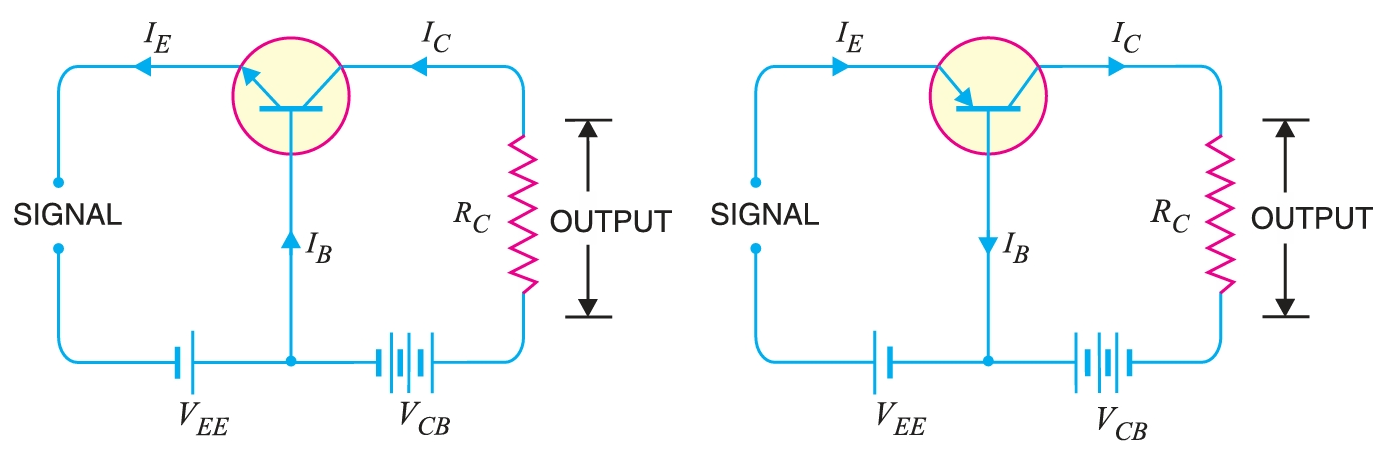
In this circuit arrangement, the input is applied between the emitter and base, and the output is taken from the collector and base. Here, the base of the transistor is common to both the input and output circuits, hence the name common-base connection. In Fig., a common base \(npn\) transistor circuit is shown, whereas Fig. shows the common base \(pnp\) transistor circuit.
Current amplification factor \( \alpha\) is the ratio of output current to input current. In a common base connection, the input current is the emitter current \(I_E\) and the output current is the collector current \(I_C\). The ratio of change in collector current to the change in emitter current at constant collector base voltage \(V_{CB}\) is known as current amplification factor, i.e., Transistors
\[\alpha = \frac{I_C}{I_E} \]
at constant \(V_{CB}\)
It is clear that the current amplification factor is less than unity. This value can be increased (but not more than unity) by decreasing the base current. This is achieved by making the base thin and doping it lightly. Practical values of \( \alpha\) in commercial transistors range from 0.9 to 0.99.
The whole of the emitter current does not reach the collector. It is because a small percentage of it, as a result of electron-hole combinations occurring in the base area, gives rise to the base current. Moreover, as the collector-base junction is reverse-biased, some leakage current flows due to minority carriers. It follows, therefore, that total collector current consists of :
- (i) That part of emitter current which reaches the collector terminal i.e. \( \alpha\) IE.
- (ii) The leakage current \(I_{\text{leakage}}\). This current is due to the movement of minority carriers across the base-collector junction on account of it being reverse-biased. This is generally much smaller than \( \alpha ~I_E\) .
\( \therefore\) Total collector current, \[I_C = \alpha ~I_E + I_{\text{leakage}}\]
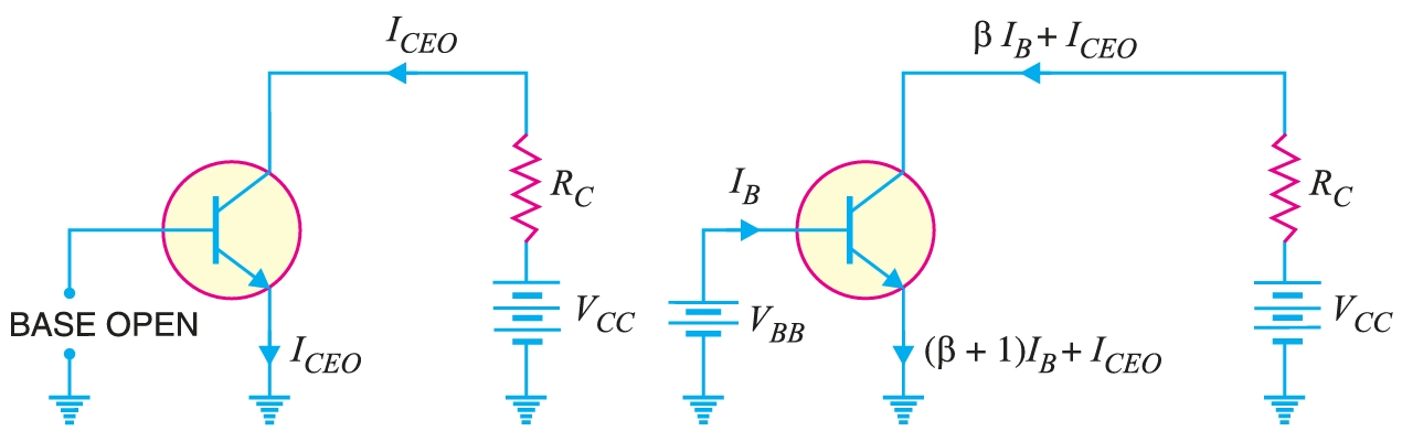
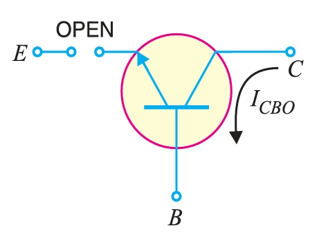
It is clear that if \(I_E = 0\) (i.e., emitter circuit is open), a small leakage current still flows in the collector circuit. This \(I_{\text{leakage}}\) is abbreviated as \(I_{CBO}\), meaning collector-base current with emitter open. The \(I_{CBO}\) is indicated in Fig. \[ I_C = \alpha ~I_E + I_{CBO}\] \[ I_E = I_C + I_{B}\] \[ I_C = \alpha ~(I_C + I_{B}) + I_{CBO}\] \[ I_C (1 - \alpha) = \alpha~I_{B} + I_{CBO}\] \[ I_C = \frac{\alpha}{(1 - \alpha)}~I_{B} + \frac{I_{CBO}}{(1 - \alpha)}\]
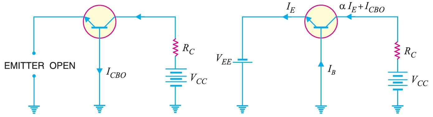
These relations can be used to find \(I_C\). The collector current of a transistor can be controlled by either the emitter or base current. Fig. shows the concept of \(I_{CBO}\). In CB configuration, a small collector current flows even when the emitter current is zero. This is the leakage collector current (i.e. the collector current when emitter is open) and is denoted by \(I_{CBO}\). When the emitter voltage \(V_{EE}\) is also applied, the various currents are as shown in Fig.
Characteristics of Common Base Connection
The complete electrical behaviour of a transistor can be described by stating the interrelation of the various currents and voltages. These relationships can be conveniently displayed graphically, and the resulting curves are known as the characteristics of a transistor. The most important characteristics of a common-base connection are the input and output characteristics.
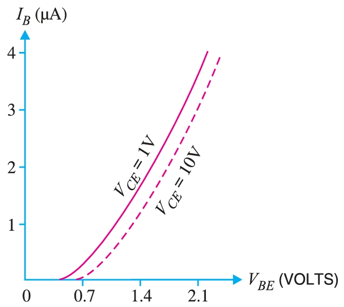
Input characteristics
It is the curve between emitter current IE and emitter-base voltage \(V_{EB}\) at constant collector-base voltage \(V_{CB}\). The emitter current is generally taken along \(y\)-axis and emitter-base voltage along \(x\)-axis. Fig. shows the input characteristics of a typical transistor in CB arrangement. The following points may be noted from these characteristics:
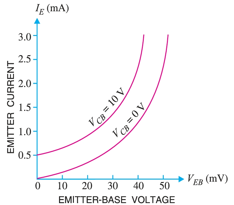
- (i) The emitter current \(I_E\) increases rapidly with small increase in emitter-base voltage \(V_{EB}\). It means that the input resistance is very small.
- (ii) The emitter current is almost independent of collector-base voltage \(V_{CB}\). This leads to the conclusion that the emitter current (and hence the collector current) is almost independent of the collector voltage.
Input resistance is the ratio of change in emitter-base voltage \( \Delta~V_{EB}\) to the resulting change in emitter current \( \Delta~I_E\) at constant collector-base voltage \(V_{CB}\), i.e., Input resistance, \[r_i = \frac{\Delta~V_{BE}}{\Delta~I_E}\] at constant \(V_{CB}\). In fact, input resistance is the opposition offered to the signal current. As a very small \(V_{BE}\) is sufficient to produce a large flow of emitter current \(I_E\), therefore, input resistance is quite small, of the order of a few ohms.
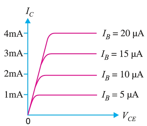
Output characteristics
It is the curve between collector current \(I_C\) and collector-base volt age \(V_{CB}\) at *constant emitter current \(I_E\). Generally, collector current is taken along \(y\)-axis and collector-base voltage along \(x\)-axis. The figure shows the output characteristics of a typical transistor in a CB arrangement. The following points may be noted from the characteristics :
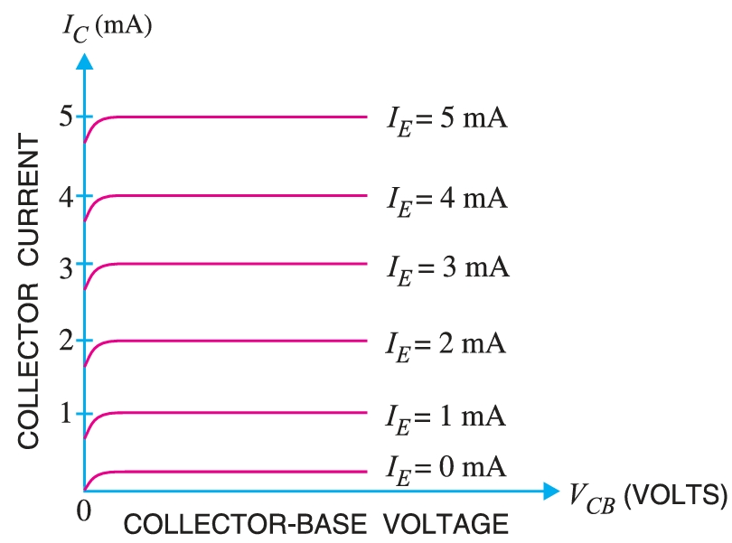
- (i) The collector current \(I_C\) varies with \(V_{CB}\) only at very low voltages (\(\lt 1~V\)). The transistor is never operated in this region.
- (ii) When the value of \(V_{CB}\) is raised above 1 - 2 V, the collector current be comes constant as indicated by straight horizontal curves. It means that now \(I_C\) is independent of \(V_{CB}\) and depends upon \(I_E\) only. This is consistent with the theory that the emitter current flows almost entirely to the collector terminal. The transistor is always operated in this region
- (iii) A very large change in collector-base voltage produces only a tiny change in collector current. This means that output resistance is very high. Output resistance. It is the ratio of change in collector-base voltage \( \Delta~V_{CB}\) to the resulting change in collector current \( \Delta~I_C\) at constant emitter current i.e., Output resistance,
\[ro = \frac{\Delta~V_{CB}}{\Delta~I_C} \]
at constant \(I_E\)
The output resistance of the CB circuit is very high, of the order of several tens of kilo-ohms. This is not surprising because the collector current changes very slightly with the change in \(V_{CB}\).
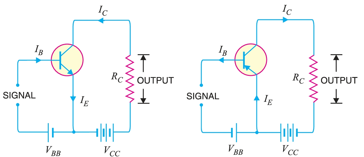
Common Emitter Connection
In this circuit arrangement, input is applied between the base and emitter, and output is taken from the collector and emitter. Here, the emitter of the transistor is common to both the input and output circuits, and hence the name common emitter connection. Fig. shows common emitter \(npn\) transistor circuit whereas Fig. shows common emitter \(pnp\) transistor circuit
Base current amplification factor \( \beta\).
In a common emitter connection, the input current is \(I_B\) and the output current is \(I_C\). The ratio of change in collector current \(\Delta~I_C\) to the change in base current \(\Delta~I_B\) is known as base current amplification factor i.e. \[\beta = \frac{\Delta~I_C}{\Delta~I_B}\]
In almost any transistor, less than 5% of emitter current flows as the base current. Therefore, the value of \( \beta\) is generally greater than 20. Usually, its value ranges from 20 to 500. This type of connection is frequently used because it provides appreciable current and voltage gains.
A simple relation exists between \( \beta\) and \(\alpha\) which can be derived, given below: \[\alpha = \frac{\Delta~I_C}{\Delta~I_E}\] and \[\beta = \frac{\Delta~I_C}{\Delta~I_B}\] Now, \[I_E = I_B + I_C\] or \[\Delta~I_E = \Delta~I_B + \Delta~I_C\] or \[\Delta~I_B = \Delta~I_E - \Delta~I_C\] Substituting the value of \(\Delta~I_B\) in equation of \(\beta\), we have, \[\beta = \frac{\Delta~I_C}{\Delta~I_E - \Delta~I_C}\] or \[\beta = \frac{\frac{\Delta~I_C}{\Delta~I_E}}{\frac{\Delta~I_E}{\Delta~I_E} - \frac{\Delta~I_C}{\Delta~I_E}} = \frac{\alpha}{1-\alpha}\] \[\therefore \qquad \beta = \frac{\alpha}{1-\alpha}\] or \[\beta + 1 = \frac{1}{1-\alpha}\]
As \(\alpha\) approaches unity, \(\beta\) approaches infinity. In other words, the current gain in a common emitter connection is very high. This is why this circuit arrangement is used in about 90 to 95 percent of all transistor applications.
In common emitter circuit, \(I_B\) is the input current and \(I_C\) is the output current. \[ I_C = \alpha ~I_E + I_{CBO}\] \[ I_E = I_C + I_{B}\] \[ I_C = \alpha ~(I_C + I_{B}) + I_{CBO}\] \[ I_C (1 - \alpha) = \alpha~I_{B} + I_{CBO}\] \[ I_C = \frac{\alpha}{(1 - \alpha)}~I_{B} + \frac{I_{CBO}}{(1 - \alpha)}\] From the expression, if \(I_B =0\) (i.e. base circuit is open), the collector current will be the current to the emitter. This is abbreviated as \(I_{CEO}\), meaning collector-emitter current with base open. \[ I_{CEO} = \frac{1}{(1 - \alpha)}I_{CBO}\] or \[ I_{CEO} = (\beta+1)~I_{CBO}\] Then, we the expression of \(I_C\) becomes \[ I_C = \beta~I_{B} + I_{CEO}\] In CE configuration, a small collector current flows even when the base current is zero. This is the collector cut off current (i.e. the collector current that flows when base is open) and is denoted by \(I_{CEO}\). The value of \(I_{CEO}\) is much larger than \(I_{CBO}\).