Transistor Biasing
The basic function of a transistor is to do amplification. A weak signal is applied to the base of the transistor, and an amplified output is obtained at the collector. One important requirement during amplification is that only the signal magnitude should increase, with no change in signal shape. This increase in signal magnitude without any change in shape is known as faithful amplification. To achieve this, the method ensures that the input circuit (i.e., base-emitter junction) of the transistor remains forward-biased and the output circuit (i.e., collector-base junction) remains reverse-biased throughout the signal. This is known as transistor biasing.
The process of raising the strength of a weak signal without any change in its general shape is known as faithful amplification.
We already know that it will function properly if its input circuit (i.e., base-emitter junction) remains forward-biased and its output circuit (i.e., collector-base junction) remains reverse-biased at all times. This is then the key factor for achieving faithful amplification. To ensure this, the following basic conditions must be satisfied :
- (a) Proper zero signal collector current
- (b) Minimum proper base-emitter voltage (VBE) at any instant
- (c) Minimum proper collector-emitter voltage (VCE) at any instant
The conditions (a) and (b) ensure that the base-emitter junction shall remain properly forward-biased during all parts of the signal. On the other hand, condition (c) ensures that the base-collector junction shall remain properly reverse-biased at all times. In other words, the fulfilment of these conditions ensures that the transistor operates in the active region of its output characteristics, i.e., between saturation and cutoff.
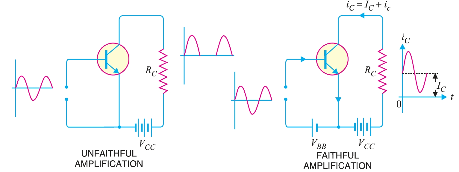
Consider an \(npn\) transistor circuit shown in Fig. 1. During the positive half-cycle of the signal, the base is positive with respect to the emitter, and hence the base-emitter junction is forward-biased. This will cause a base current and much larger collector current to flow in the circuit. The result is that the positive half-cycle of the signal is amplified in the collector as shown. However, during the negative half-cycle of the signal, the base-emitter junction is reverse-biased, so no current flows in the circuit. The result is that there is no output due to the negative half-cycle of the signal. Thus, we shall obtain an amplified signal with its negative half-cycles completely cut off, which is an unfaithful amplification.
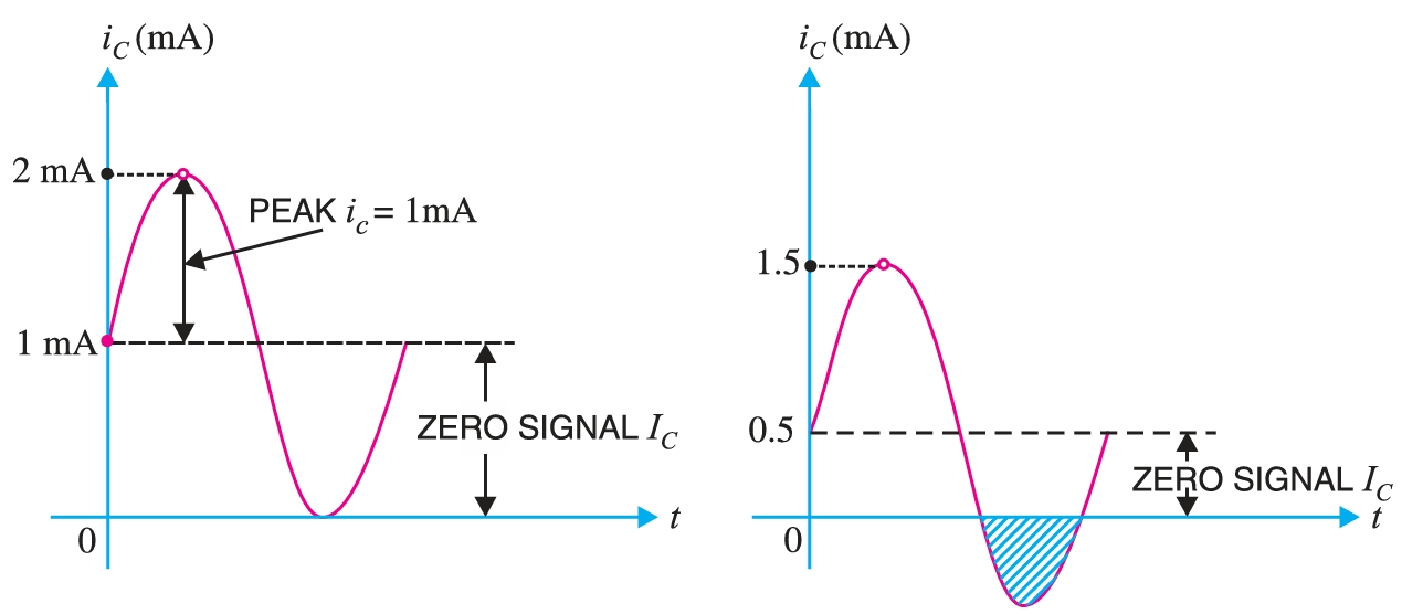
Now, introduce a battery source \(V_{BB}\) in the base circuit as shown in Fig. 1. The magnitude of this voltage should be such that it keeps the input circuit forward biased even during the peak of the negative half-cycle of the signal. When no signal is applied, a d.c. The current \(I_{C}\) will flow in the collector circuit due to \(V_{BB}\). This is known as zero signal collector current, \(I_{C-\text{zero}}\). During the positive half-cycle of the signal, the input circuit is more forward-biased and hence the collector current increases. However, during the negative half-cycle of the signal, the input circuit is less forward-biased, and the collector current decreases. In this way, the negative half-cycle of the signal also appears in the output, resulting in faithful amplification. It follows, therefore, that for faithful amplification, proper zero signal collector current must flow. The value of zero signal collector current should be at least equal to the maximum collector current due to the signal alone, i.e
\[\text{Zero signal collector current} \ge \text{Max. collector current due to the signal alone}\]
Suppose a signal applied to the base of a transistor produces a peak collector current of \(1 \,\text{mA}\). Then zero signal collector current must be at least equal to \(1 \,\text{mA}\) so that even during the peak of negative half-cycle of the signal, there is no cut off as shown in Fig. 2. If zero signal collector current is less, say, \(0.5 \,\text{mA}\) as shown in Fig. 2, then some part (shaded portion) of the negative half-cycle of signal will be cut off in the output.
In order to achieve faithful amplification, the base-emitter voltage \((V_{BE})\) should not fall below \(0.5 \,\text{V}\) for germanium transistors and \(0.7 \,\text{V}\) for \(Si\) transistors at any instant. The base current is very small until the input voltage overcomes the potential barrier at the base-emitter junction. The value of this potential barrier is \(0.5 \,\text{V}\) for \(Ge\) transistors and \(0.7 \,\text{V}\) for \(Si\) transistors. Once the potential barrier is overcome, the base current and hence the collector current increase sharply. Therefore, if base-emitter voltage VBE falls below these values during any part of the signal, that part will be amplified to a lesser extent due to a small collector current. This will result in unfaithful amplification. For faithful amplification, the collector-emitter voltage \(V_{CE}\) should not fall below \(0.5 \,\text{V}\) for \(Ge\) transistors and \(1\,\text{V}\) for silicon transistors. This is called knee voltage.
When \(V_{CE}\) is too low (less than \(0.5 \,\text{V}\) for \(Ge\) transistors and \(1 \,\text{V}\) for \(Si\) transistors), the collector base junction is not properly reverse biased. Therefore, the collector cannot attract the charge carriers emitted by the emitter, and hence a greater portion of them goes to the base. This decreases the collector current while increasing the base current. Hence, the value of \(\beta\) falls. Therefore, if \(V_{CE}\) is allowed to fall below \(V_{\text{knee}}\) during any part of the signal, that part will be less amplified due to reduced \(\beta\). This will result in unfaithful amplification. However, when \(V_{CE}\) is greater than \(V_{\text{knee}}\), the collector-base junction is properly reverse-biased, and the value of \(\beta\) remains constant, resulting in faithful amplification. It is the fulfilment of these conditions which is known as transistor biasing.
The proper flow of zero signal collector current and the maintenance of proper collector-emitter voltage during the passage of a signal is known as transistor biasing.
Methods of Transistor Biasing
The following are the most commonly used methods of obtaining transistor biasing from one source of supply (i.e., \(V_{CC}\) ) :
- (a) Fixed-bias method or Base resistor method
- (b) Emitter bias method
- (c) Voltage-divider bias
Fixed-bias method
In this method, a high resistance \(R_{B}\) (several hundred \(\text{k}\Omega\)) is connected between the base and positive end of supply for \(npn\) transistor and between the base and negative end of supply for the \(pnp\) transistor. Here, the required zero signal base current is provided by \(V_{CC}\), and it flows through \(R_{B}\). This is because the base is now positive with respect to the emitter, i.e., the base-emitter junction is forward-biased. The required zero-signal base current \(I_{B}\) (and hence \(I_{C} = \beta I_{B}\)) can be achieved by selecting the proper value of base resistor \(R_{B}\).
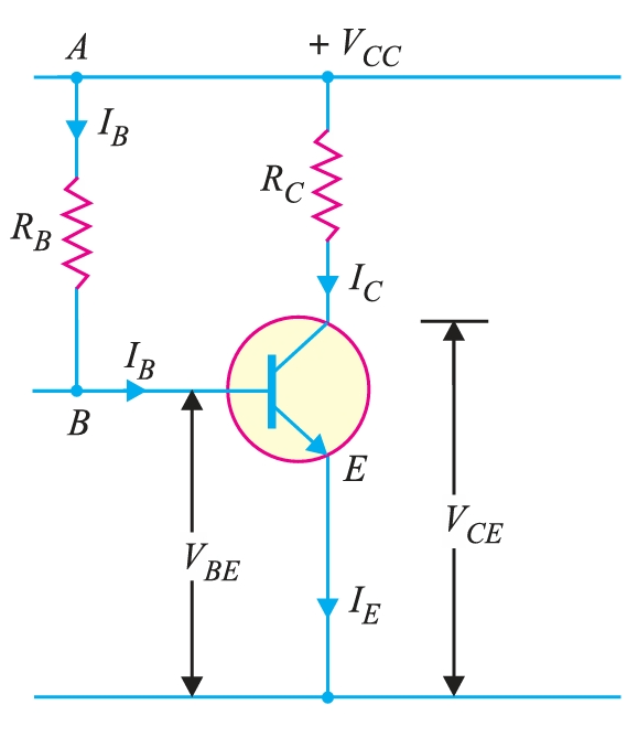
It is required to find the value of \(R_{B}\) so that the required collector current flows in the zero signal conditions. Let \(I_{C}\) be the required zero signal collector current.
\[\therefore \quad I_B = \frac{I_C}{\beta}\]
Considering the closed circuit ABENA and applying Kirchhoff's voltage law, we get,
\[V_{CC}= I_{B}R_{B}+V_{BE}\] or \[I_{B}R_{B}= V_{CC}-V_{BE}\] \[\therefore R_{B} = \frac{V_{CC}-V_{BE}}{I_{B}}\]
As \(V_{CC}\) and \(I_{B}\) are known, and \(V_{BE}\) can be seen from the transistor manual, therefore, the value of \(R_{B}\) can be readily found. Since \(V_{BE}\) is generally quite small as compared to \(V_{CC}\), the former can be neglected with little error. \[R_{B} = \frac{V_{CC}}{I_{B}}\] \(V_{CC}\) is a fixed known quantity, and \(I_{B}\) is chosen at some suitable value. Hence, \(R_{B}\) can always be found directly, and for this reason, this method is sometimes called the fixed-bias method.
Advantages
- This biasing circuit is very simple, as only one resistance, \(R_{B}\), is required.
- Biasing conditions can easily be set, and the calculations are simple.
- There is no loading of the source by the biasing circuit since no resistor is employed across the base-emitter junction.
Disadvantages
- This method provides poor stabilisation. It is because there is no means to stop a self-increase in collector current due to temperature rise and individual variations. For example, if \(\beta\) increases due to transistor replacement, then IC also increases by the same factor as \(I_B\) is constant.
- The stability factor is very high. Therefore, there is a high risk of thermal runaway. Due to these disadvantages, this biasing method is rarely employed.
Emitter Bias Method
Fig. shows the emitter bias circuit. This circuit differs from the base-bias circuit in two important respects. First, it uses two separate d.c. voltage sources; one positive \((+ V_{CC})\) and the other negative \((– V_{EE})\). Normally, the two supply voltages will be equal. For example, if \(V_{CC} = + 20\,\text{V}\) (d.c.), then \(V_{EE} = – 20\,\text{V}\) (d.c.). Secondly, there is a resistor \(R_{E}\) in the emitter circuit.
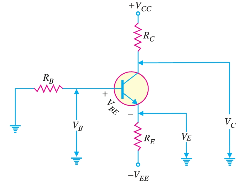
Fig. shows the emitter bias circuit. The following method is used to find the \(Q\)-point values (i.e., d.c. \(I_{C}\) and d.c. \(V_{CE}\)) for this circuit.
Applying Kirchhoff’s voltage law to the base-emitter circuit, we have, \[-I_{B}R_{B} - V_{BE}- I_{E}R_{E} + V_{EE} =0\] \[\therefore V_{EE} = I_{B}R_{B} + V_{BE} + I_{E}R_{E}\] Now, \[I_{C} \simeq I_{E} \,\text{and}\, I_{C}=\beta I_{B}\] \[\therefore I_B \simeq \frac{I_{E}}{\beta}\] and putting all these in the above equations, we have,
\[V_{EE} = \left(\frac{I_{E}}{\beta}\right)R_{B}+I_{E}R_{E}+ V_{BE}\] or \[V_{EE}- V_{BE} = \left(\frac{I_{E}}{\beta}\right)R_{B}+I_{E}R_{E}\] \[\therefore \quad I_{C} \simeq I_{E} = \frac{V_{EE}- V_{BE}}{R_{E}+\frac{R_{B}}{\beta} }\] or \[\boxed{I_{C} = \frac{V_{EE}- V_{BE}}{R_{E}+\frac{R_{B}}{\beta} }}\]
Fig. shows the various voltages of the emitter bias circuit with respect to ground
Emitter voltage w.r.t. ground is
\[V_{E} = -V_{EE} + I_{E}R_{E}\]
Base voltage w.r.t. ground is \[V_{B} = V_{E} + V_{BE}\] Collector voltage w.r.t. ground is \[V_{C} = V_{CC} - I_{C}R_{C}\] Subtracting \(V_{E}\) from \(V_{C}\) and using the approximation \(I_{C} \simeq I_{E}\), we have, \[V_{C} – V_{E} = (V_{CC} – I_{C} R_{C}) – (– V_{EE} + I_{C} R_{E})\] or \[V_{CE} = V_{CC} + V_{EE} – I_{C} (R_{C} + R_{E})\]
Emitter biasing is another common method used to stabilize the operating point of a transistor amplifier. It involves connecting a resistor in the emitter leg and often using a negative supply voltage for the base bias.
Advantages
- The emitter resistor provides negative feedback, which helps stabilize the operating point against temperature variations.
- The bias point is less sensitive to transistor parameter changes, making circuits more reliable across different devices.
- Requires fewer components compared to voltage divider biasing, making it easier to implement in some cases.
- Any increase in collector current raises the emitter voltage, which reduces base-emitter voltage and counteracts the increase.
Disadvantages
- Often needs both positive and negative supply voltages, which complicates the design compared to single-supply biasing methods.
- The emitter resistor introduces negative feedback, which stabilizes the circuit but lowers the overall voltage gain.
- Because of the need for dual supplies, it is not as widely used as voltage divider biasing in modern amplifier designs.
- Continuous current through the emitter resistor leads to wasted power.
Voltage Divider Bias Method
The Voltage Divider Bias Method is the most widely used method of providing biasing and stabilisation to a transistor. In this method, two resistances, \(R_{1}\) and \(R_{2}\), are connected across the supply voltage \(V_{CC}\) and provide biasing. The emitter resistance \(R_{E}\) provides stabilisation. The name ‘‘voltage divider’’ comes from the voltage divider formed by \(R_{1}\) and \(R_{2}\). The voltage drop across \(R_{2}\) forward biases the base-emitter junction. This causes the base current and hence the collector current to flow in the zero signal conditions.
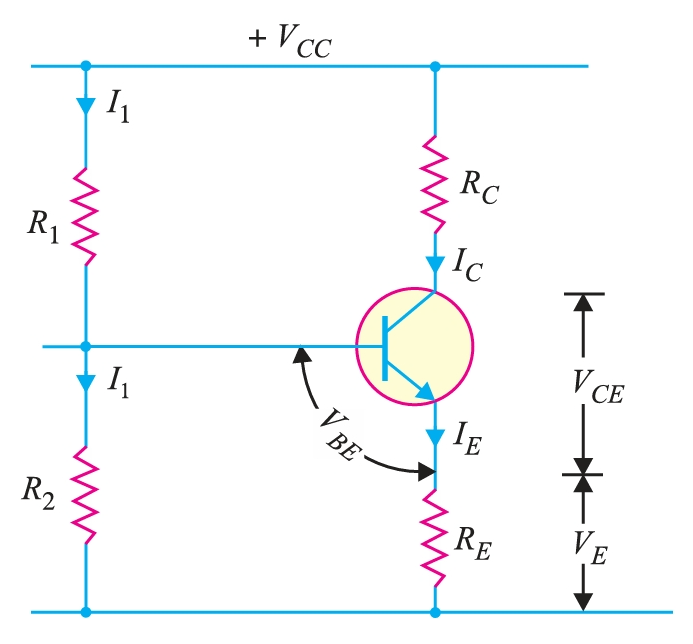
Suppose that the current flowing through resistance \(R_{1}\) is \(I_{1}\). As the base current \(I_{B}\) is very small, it can be assumed with reasonable accuracy that the current flowing through \(R_{2}\) is also \(I_{1}\).
\[I_{1} = \frac{V_{CC}}{R_{1} + R_{2}}\] therefore Voltage across resistance \(R_{2}\) is \[V_{2} = \left(\frac{V_{CC}}{R_{1} + R_{2}}\right)R_{1}\] Applying Kirchhoff's voltage law to the base circuit \[V_{2} = V_{BE} + V_{E}\] or \[V_{2} = V_{BE} + I_{E}R_{E}\] or \[I_{E}= \frac{V_{2} - V_{BE}}{R_{E}} \] \[\therefore \quad I_{C} \simeq \frac{V_{2} - V_{BE}}{R_{E}} \]
\(I_{C}\) does not at all depend upon \(\beta\). Though \(I_{C}\) depends upon \(V_{BE}\) but in practice \(V_{2} \gg V_{BE}\) so that \(I_{C}\) is practically independent of \(V_{BE}\). Thus, \(I_{C}\) in this circuit is almost independent of the transistor parameters, ensuring good stabilisation. This is why potential divider bias has become a universal method for transistor biasing.
Applying Kirchhoff's voltage law to the collector side, \[V_{CC} = I_{C} R_{C} + V_{CE} + I_{E} R_{E}\]
\[V_{CC} = I_{C} R_{C} + V_{CE} + I_{C} R_{E} \quad \because I_{E} \simeq I_{C})\] \[V_{CC} = I_{C} (R_{C} + R_{E}) + V_{CE} \] \[V_{CE} = V_{CC} - I_{C} (R_{C} + R_{E})\]
Voltage divider biasing is one of the most widely used methods for biasing a transistor amplifier. It uses two resistors in series across the supply voltage to provide a stable bias point.
Advantages
- The operating point (\(Q\)-point) is less affected by changes in transistor current gain (\(\beta\)), making it reliable across different transistors.
- Provides good stability against temperature variations, reducing the risk of thermal runaway.
- Because of its reliability, it is the most common biasing method in amplifier circuits.
- Easy to implement with just two resistors forming the divider.
Disadvantages
- The biasing resistors continuously draw current, leading to wasted power.
- Since part of the supply voltage is dropped across the biasing resistors, the available voltage swing for the output is limited.
- Choosing resistor values involves balancing stability and power efficiency, which can be tricky.
- The continuous current through the divider makes it less efficient in battery-operated devices.
Operational Regions
Fig. shows the output characteristics of a \(CE\) mode transistor along with the d.c. load line.
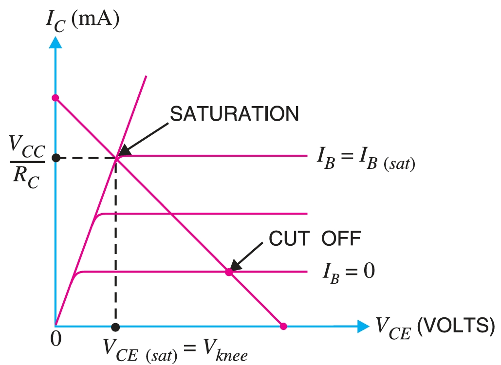
Cut off
The point where the load line intersects the \(I_{B} = 0\) curve is known as the cut-off. At this point, \(I_{B} = 0\) and only a small collector current (i.e., collector leakage current \(I_{CEO}\)) exists. At cut-off, the base-emitter junction no longer remains forward-biased, and normal transistor action is lost. The collector-emitter voltage is nearly equal to \(V_{CC}\), i.e.,
\[V_{CE(cut-off)} = V_{CC}\]
Saturation
The point where the load line intersects the \(I_B = I_{B(\text{sat})}\) curve is called saturation. At this point, the base current is maximum, and so is the collector current. At saturation, the collector base junction no longer remains reverse-biased, and normal transistor action is lost.
\[I_{C(\text{sat})} \simeq \frac{V_{CC}}{R_{C}}\]
\[V_{CE} = V_{CE(\text{sat})} = V_{knee}\]
If the base current is greater than \(I_{B(\text{sat})}\), then the collector current cannot increase because the collector-base junction is no longer reverse-biased.
Active region
The region between cutoff and saturation is known as the active region. In the active region, the collector-base junction remains reverse-biased while the base-emitter junction remains forward-biased. Consequently, the transistor will function normally in this region. The transistor is biased to operate in the active region.
A transistor has two \(pn\) junctions, i.e., it is like two diodes. The junction between base and emitter may be called emitter diode. The junction between the base and the collector may be called a collector diode.
The transistor can be in one of three states: cut-off, saturated, or active. The state of a transistor is entirely determined by the states of the emitter diode and collector diode. The relations between the diode states and the transistor states are :
- CUT-OFF : Emitter diode and collector diode are OFF.
- ACTIVE : Emitter diode is ON and collector diode is OFF.
- SATURATED : Emitter diode and collector diode are ON.
In the active state, collector current is \(\beta\) times the base current (i.e., \(I_{C} = \beta I_{B}\)). If the transistor is cut off, there is no base current, so there is no collector or emitter current. That is, the collector-emitter pathway is open. In saturation, the collector and emitter are effectively shorted together. That is, the transistor behaves as though a switch has been closed between the collector and emitter. When the transistor is in the active state, \(I_{C} = \beta I_{B}\). Therefore, a transistor acts as an amplifier when operating in the active state.