Small Signal Amplifier
Under Preparation
Cascade Amplifier
A transistor circuit containing more than one stage of amplification is known as a cascade or multi-stage transistor amplifier. A number of single amplifiers are connected in a cascade arrangement, i.e., the output of the first stage is connected to the input of the second stage through a suitable coupling device, and so on. The purpose of the coupling device (e.g., a capacitor, transformer, etc.) is to transfer a.c. output of one stage to the input of the next stage, and to isolate the d.c. conditions of one stage from the next stage. Each stage consists of a single transistor and associated circuitry and is coupled to the next stage via a coupling device.
A capacitor is used as the coupling device in RC coupling. The capacitor connects the output of one stage to the input of the next stage in order to pass the a.c. signal on while blocking the d.c. bias voltages. A transformer is used as the coupling device in transformer coupling. The transformer coupling provides the same two functions (viz., to pass the signal on and block d.c.) but also permits impedance matching. The individual amplifier-stage bias conditions are so designed that the two stages may be directly connected without the necessity for d.c. coupling. isolation in direct coupling or d.c. coupling.
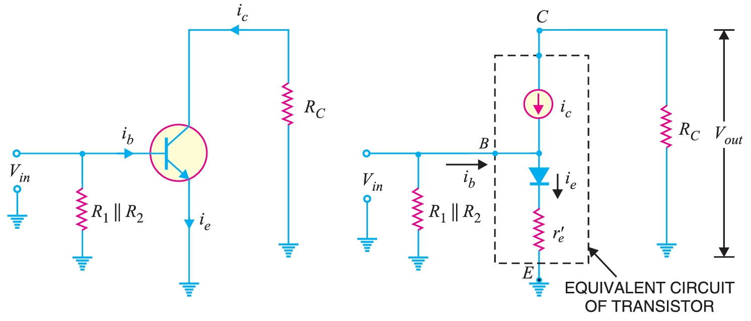
A capacitor blocks d.c. i.e., a capacitor behaves as an ``open'' to d.c. Therefore, the capacitors are removed from the transistor amplifier circuit for d.c. analysis. A capacitor offers reactance \((= 1/2\pi fC) \) to a.c. depending upon the values of \(f\) and \(C\). In practical transistor circuits, the size of capacitors is so selected that they offer negligible (ideally zero) reactance to the range of frequencies handled by the circuits. Therefore, for a.c. analysis, we can replace the capacitors with a short.
The capacitors are commonly used to connect one amplifier stage to another. When a capacitor is used for this purpose, it is called a coupling capacitor. A coupling capacitor performs the following two functions :
- (i) It blocks d.c. or it provides D.C. isolation between the two stages of a multistage amplifier.
- (ii) It passes the a.c. signal from one stage to the next with little or no distortion.
A bypass capacitor also blocks d.c. and behaves as a short or wire due to the proper selection of capacitor size to an a.c. signal. A bypass capacitor is connected in parallel with a circuit component (e.g. resistor) to bypass the a.c. signal.
Gain
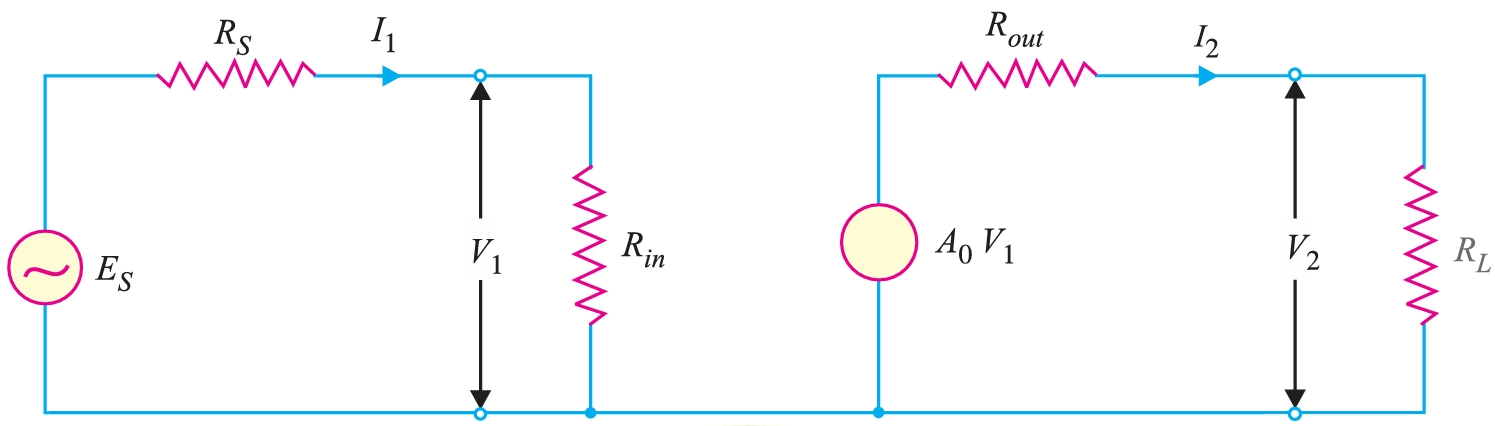
The ratio of the output electrical quantity to the input of the amplifier is called its gain. The gain of a multistage amplifier is equal to the product of the gains of individual stages. For example, if the individual voltage gain of a three-stage amplifier is \(A_{v1}\), \(A_{v2}\), and \(A_{v3}\), and the total voltage gain \(A_{\text{network}}\) is
\[A_{\text{network}} = A_{v1} \times A_{v2} \times A_{v3}\]
However, the total gain \(A_{\text{network}}\) is less than \(A_{v1} \times A_{v2} \times A_{v3}\) due to the loading effect of next stages.
Decibel
The gain is a dimensionless quantity. In practice, the gain of an amplifier is expressed in Bel or deciBel (dB).
The common logarithm (log to the base 10) of power gain is known as bel power gain.
\[\,\text{Power Gain}\, = \log_{10}\frac{P_{out}}{P_{in}} \, \text{Bel}\]
\[1 \, \text{Bel} = 10 \, \text{dB}\]
Hence,
\[\,\text{Power Gain}\, = 10 \, \log_{10}\frac{P_{out}}{P_{in}} \, \text{dB}\]
So, the voltage gain in \(\text{dB}\) for equal resistances can be expressed as
\[A_{v} = 20 \, \log_{10}\frac{V_{out}}{V_{in}} \, \text{dB}\]
When the gains are expressed in \(\text{dB}\), the overall gain of a multistage amplifier is the sum of the gains of individual stages in \(\text{dB}\). Also, the natural response of human ears is logarithmic, which matches the loudness of the sound. In other words, the intensity of sound given by the speaker (i.e., power) is increased 100 times, and our ears hear a doubling effect \((\log_{10} 100 = 2)\)
Frequency response
The voltage gain of an amplifier varies with signal frequency. This is because the reactance of the capacitor in the circuit changes with signal frequency, thereby affecting the output voltage. The curve relating the voltage gain to the signal frequency of an amplifier is known as the frequency response.
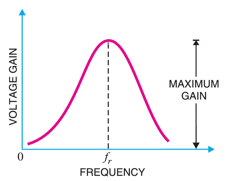
The amplifier gain increases with frequency from zero to a maximum at \(f_{r}\), called the resonant frequency. If the signal frequency exceeds \(f_{r}\), the gain decreases. The performance of an amplifier depends to a considerable extent upon its frequency response.
Bandwidth
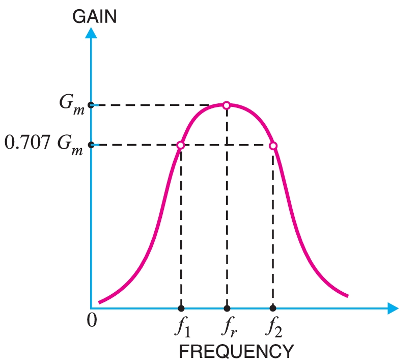
The range of frequency over which the voltage gain is equal to or greater than \(70.7 \,\% %\) of the maximum gain is known as bandwidth.
The human ear is not very sensitive. The ear cannot detect a change if the gain falls to \(70.7 \,\%\) of maximum, and hence no distortion will be heard. However, if the gain falls below \(70.7 \,\%\), the ear will hear clear distortion.
The voltage gain of an amplifier changes with frequency. The gain is equal to or greater than \(70.7 \%\) of the maximum gain for any frequency lying between \(f_{1}\) and \(f_{2}\) (limiting frequencies). The former \((f_{1})\) is called the lower cut-off frequency, and the latter \((f_{2})\) is known as the upper cut-off frequency. Therefore, \(f_{1}-f_{2}\) is the bandwidth. The signal frequency range must be within the bandwidth of the amplifier for distortion-free amplification.
The bandwidth of an amplifier can also be defined in terms of \(\text{dB}\).
\[A_{v} = 20 \, \log_{10}\frac{1}{0.707} \, \text{dB}\]
\[A_{v} = 20 \, \log_{10} 1.4142 \, \text{dB} = 3 \, \text{dB}\]
Hence bandwidth of an amplifier is the range of frequency at the limits of which its voltage gain falls by \(3 \, \text{dB}\) from the maximum gain. The frequency \(f1\) or \(f2\) is also called \(3 \, \text{dB}\) frequency or half-power frequency. The term half-power is used because when voltage is down to \(0.707\) of its maximum value, the power (proportional to \(V^{2}\)) is down to \((0.707)^{2}\) or one-half of its maximum value.
RC Coupled Transistor Amplifier
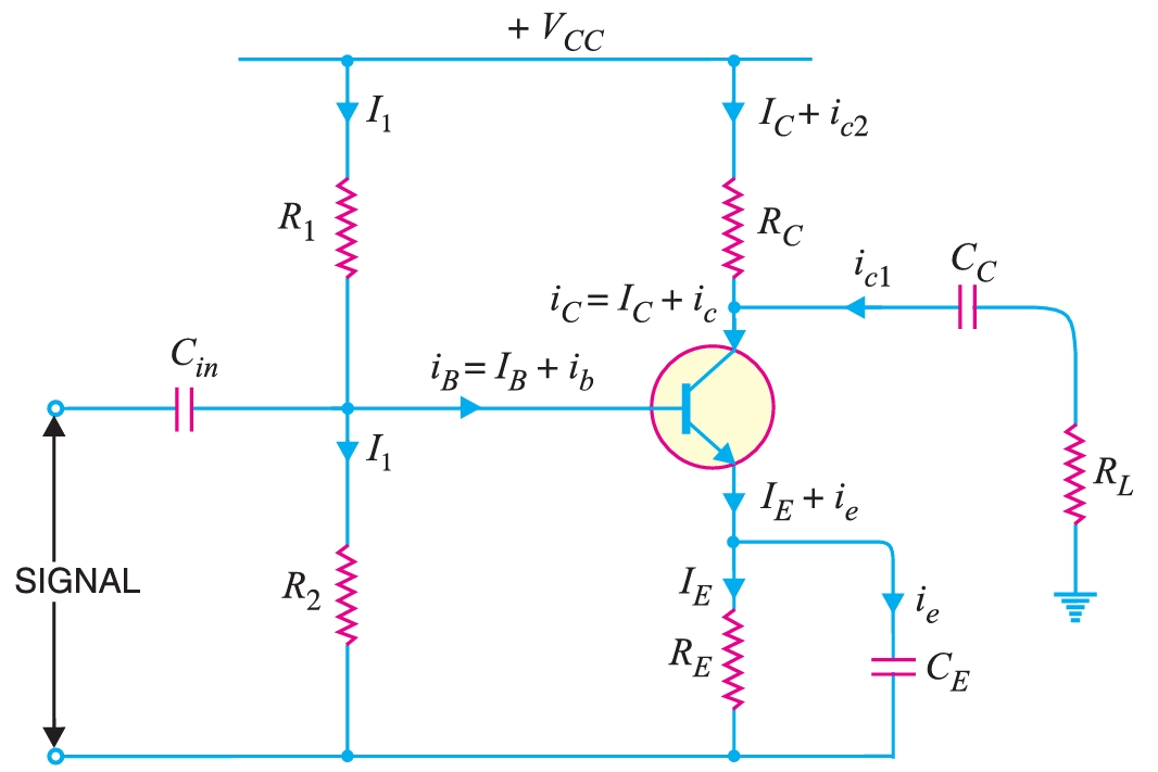
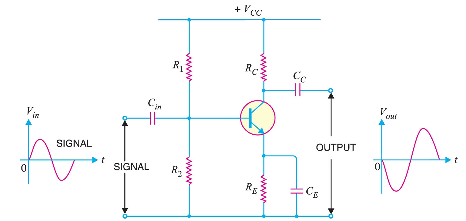
This is the most popular type of coupling because it is cheap and provides excellent audio fidelity over a wide range of frequency. It is usually employed for voltage amplification. A coupling capacitor \(C_{C}\) is used to connect the output of first stage to the base (i.e. input) of the second stage and so on.
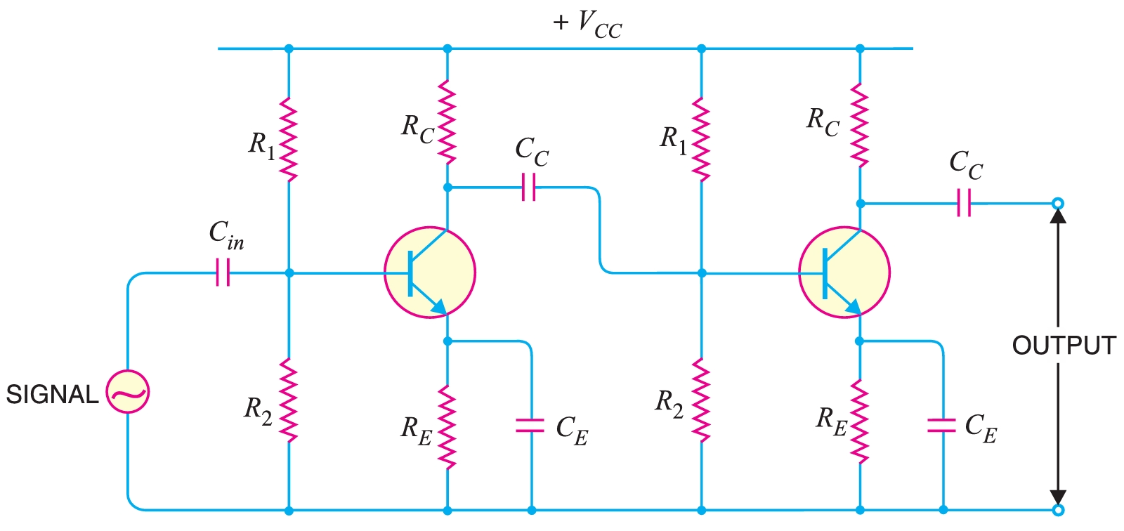
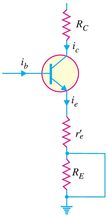
As the coupling from one stage to next is achieved by a coupling capacitor followed by a connection to a shunt resistor, therefore, such amplifiers are called resistance - capacitance coupled amplifiers. The resistances \(R_{1}\), \(R_{2}\) and \(R_{E}\) form the biasing and stabilisation network. The emitter bypass capacitor offers low reactance path to the signal. Without it, the voltage gain of each stage would be lost. The coupling capacitor \(C_{C}\) transmits a.c. signal but blocks d.c. This prevents d.c. interference between various stages and the shifting of operating point.
Advantages
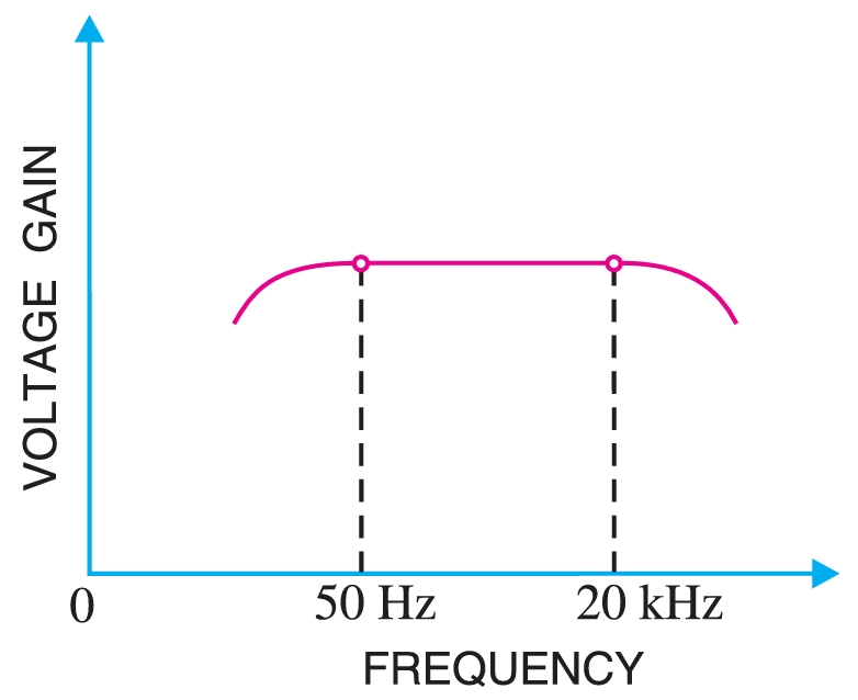
- (i) It has excellent frequency response. The gain is constant over the audio frequency range which is the region of most importance for speech, music etc.
- (ii) It has lower cost since it employs resistors and capacitors which are cheap.
- (iii) The circuit is very compact as the modern resistors and capacitors are small and extremely light.
Disadvantages
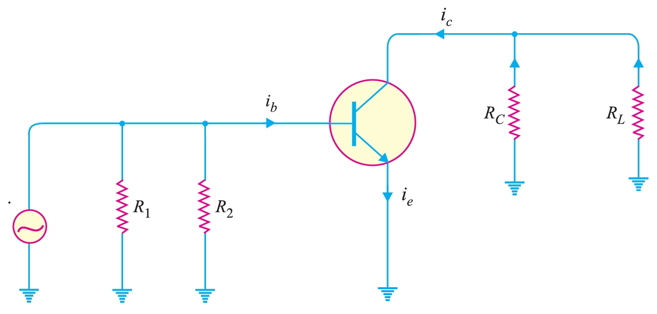
- (i) The \(RC\) coupled amplifiers have low voltage and power gain. It is because the low resistance presented by the input of each stage to the preceding stage decreases the effective load resistance \((R_{AC}) \) and hence the gain.
- (ii) They have the tendency to become noisy with age, particularly in moist climates.
- (iii) Impedance matching is poor. It is because the output impedance of RC coupled amplifier is several hundred ohms.
Transformer-Coupled Amplifier
The main reason for low voltage and power gain of RC coupled amplifier is that the effective load \((R_{AC})\) of each stage is decreased due to the low resistance presented by the input of each stage to the preceding stage. If the effective load resistance of each stage could be increased, the voltage and power gain could be increased. This can be achieved by transformer coupling. By the use of impedance-changing properties of transformer, the low resistance of a stage (or load) can be reflected as a high load resistance to the previous stage.
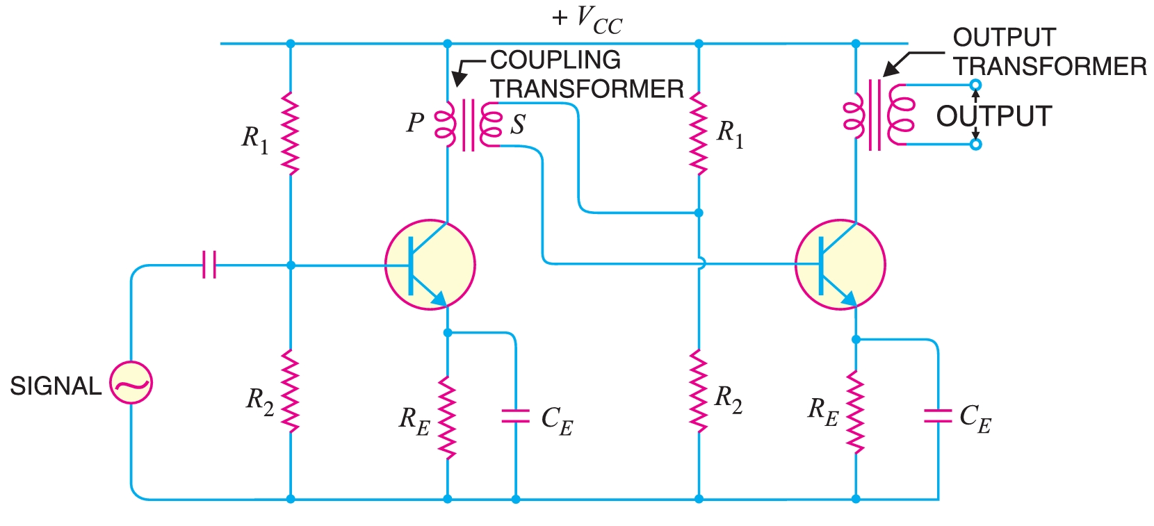
Transformer coupling is generally employed when the load is small. It is mostly used for power amplification. A coupling transformer is used to feed the output of one stage to the input of the next stage. The primary \(P\) of this transformer is made the collector load and its secondary \(S\) gives input to the next stage.
Advantages
- (i) No signal power is lost in the collector or base resistors.
- (ii) An excellent impedance matching can be achieved in a transformer coupled amplifier. It is easy to make the inductive reactance of primary equal to the output impedance of the transistor and inductive reactance of secondary equal to the input impedance of next stage.
- (iii) Due to excellent impedance matching, transformer coupling provides higher gain. As a matter of fact, a single stage of properly designed transformer coupling can provide the gain of two stages of \(RC\) coupling.
Disadvantages
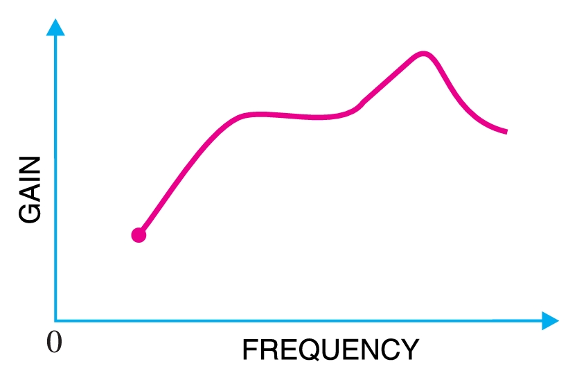
- (i) It has a poor frequency response i.e.the gain varies considerably with frequency.
- (ii) The coupling transformers are bulky and fairly expensive at audio frequencies.
- (iii) Frequency distortion is higher i.e. low frequency signals are less amplified as compared to the high frequency signals.
- (iv) Transformer coupling tends to introduce back-emf (hum voltage) in the output.
Direct-Coupled Amplifier
There are many applications in which extremely low frequency \((< 10 Hz)\) signals are to be amplified e.g. amplifying photo-electric current, thermo-couple current etc. The coupling devices such as capacitors and transformers cannot be used because the electrical sizes of these components become very large at extremely low frequencies. Under such situations, one stage is directly connected to the next stage without any intervening coupling device. This type of coupling is known as direct coupling. It uses complementary transistors. Thus, the first stage uses npn transistor, the second stage uses \(pnp\) transistor and so on. This makes the circuit stable w.r.t. temperature changes. In this connection (i.e., \(npn\) followed by \(pnp\)), the direction of collector current increase \(\beta\), when the temperature rises, is opposite for the two transistors. Thus the variation in one transistor tends to cancel that in the other. This arrangement makes the design very simple.
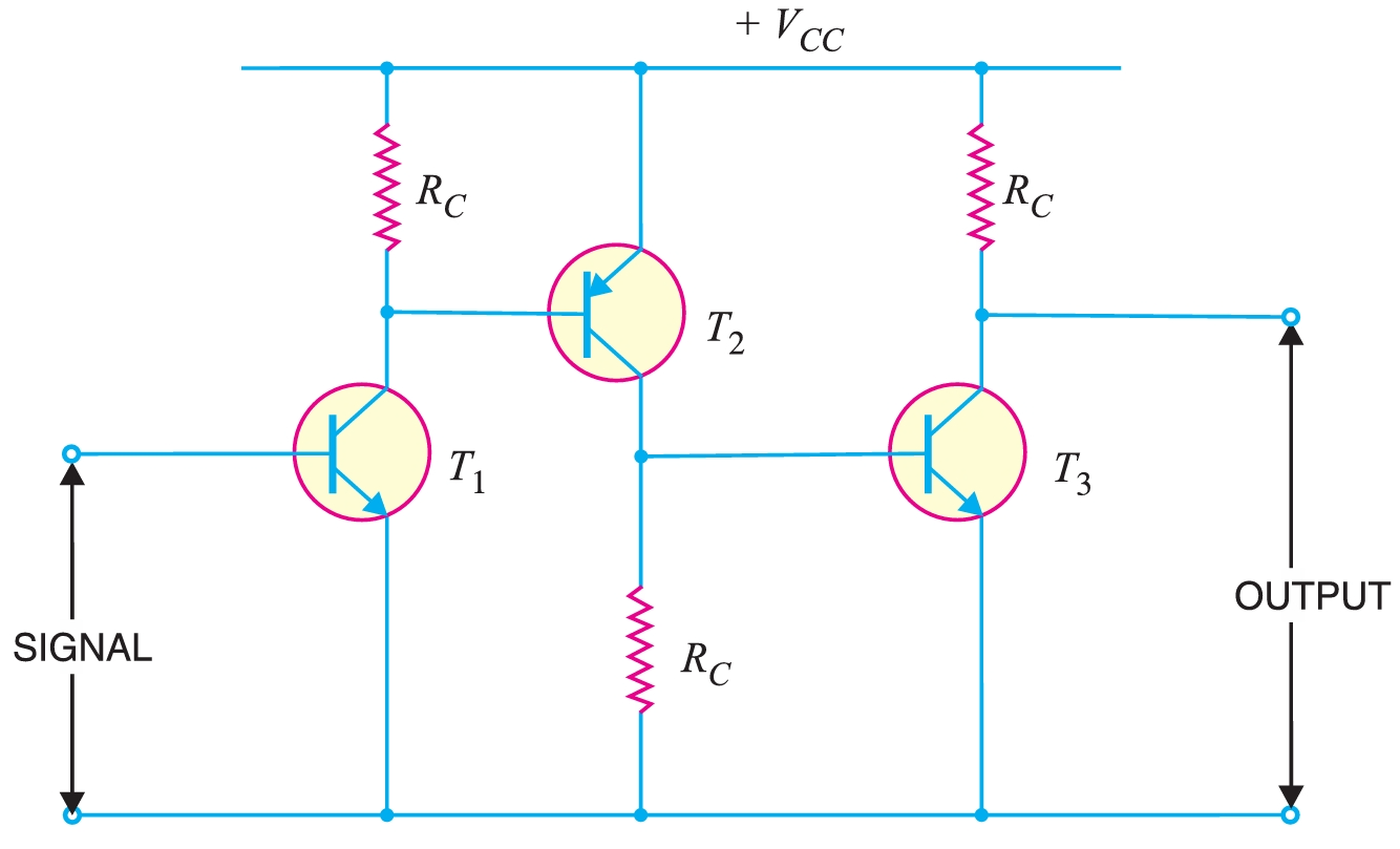
The output from the collector of first transistor \(T_{1}\) is fed to the input of the second transistor \(T_{2}\) and so on.The weak signal is applied to the input of first transistor \(T_{1}\). Due to transistor action, an amplified output is obtained across the collector load \(RC\) of transistor \(T_{1}\). This voltage drives the base of the second transistor and amplified output is obtained across its collector load. In this way, direct coupled amplifier raises the strength of weak signal.
Advantages
- (i) The circuit arrangement is simple because of minimum use of resistors.
- (ii) The circuit has low cost because of the absence of expensive coupling devices.
Disadvantages
- (i) It cannot be used for amplifying high frequencies.
- (ii) The operating point is shifted due to temperature variations.