Differential Amplifier
An amplifier circuit that accepts two input signals and amplifies the difference between these two signals. Such an amplifier is called a differential amplifier (DA). A differential amplifier is a circuit that can accept two input signals and amplify their difference.
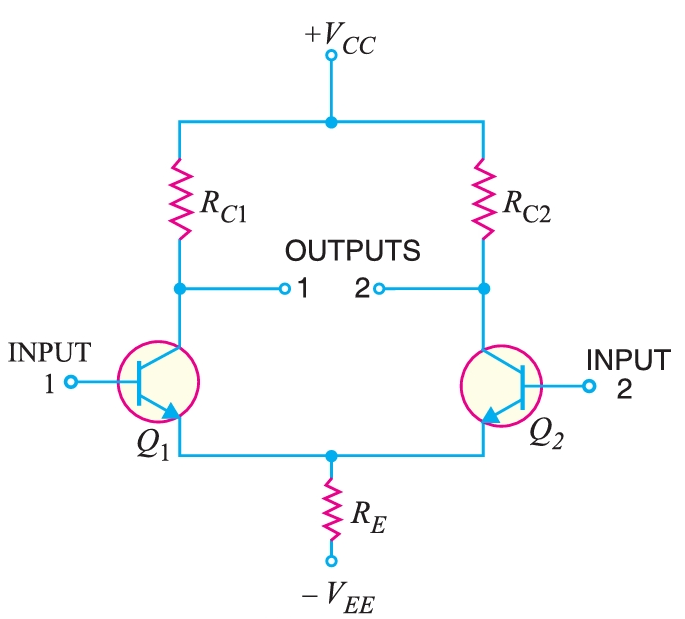
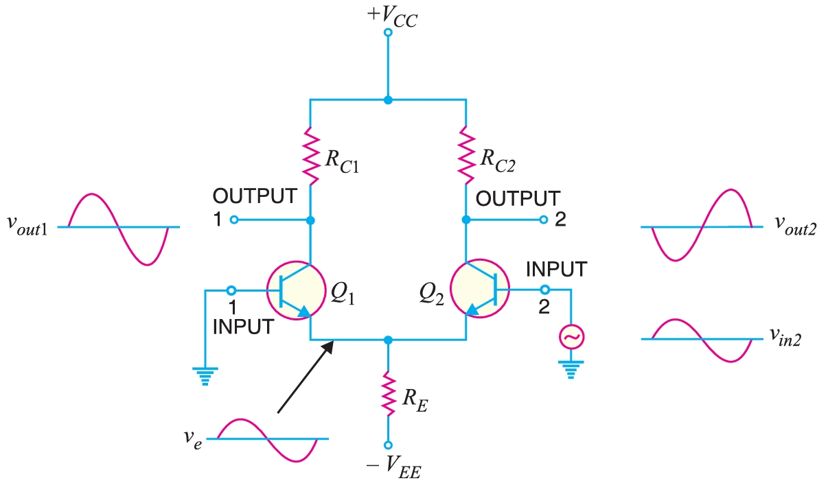
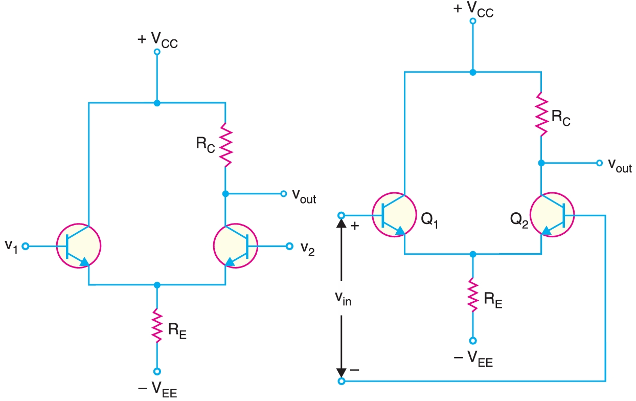
Fig. 1. shows the basic circuit of a differential amplifier. It consists of two transistors, \(Q_{1}\) and \(Q_{2}\), that have identical (ideally) characteristics. They share a common positive supply \(V_{CC}\), a common emitter resistor \(R_{E}\), and a common negative supply \(V_{EE}\). The circuit is symmetrical.
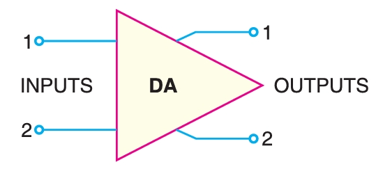
Fig. 2 shows the symbol of a differential amplifier. The important points about the differential amplifier are :
- The differential amplifier (DA) is a two-input terminal device using at least two transistors. There are two output terminals marked 1 \((v_{\text{out}\, 1} )\) and 2 \((v_{\,\text{out}\, 2})\).
- The differential amplifier transistors \(Q_{1}\) and \(Q_{2}\) are matched so that their characteristics are the same. The collector resistors (\(R_{C1}\) and \(R_{C2}\)) are also equal. The equality of the matched circuit components makes the differential amplifier circuit arrangement completely symmetrical.
- A signal is applied in two ways to a differential amplifier (DA). The signal is applied to one input of the differential amplifier, and the other input is grounded. In that case, it is called a single-ended input arrangement. The signals are applied to both differential amplifier inputs. In that case, it is called a dual-ended or double-ended input arrangement.
- The output is taken from differential amplifier in two ways. The output can be taken from one of the output terminals and the ground. In that case, it is called a single-ended output arrangement. The output can be taken between the two output terminals (i.e., between the collectors of \(Q_{1}\) and \(Q_{2}\)). In that case, it is called a double-ended output arrangement or a differential output.
Generally, the differential amplifier (DA) is operated for a single-ended output. In other words, we take the output from either output terminal \(1\) and ground or output terminal \(2\) and ground. Any grounded input/output terminal is at \(0\,\text{V}\,\).
Operation of Differential Amplifier
The signal is applied to input \(1\) (i.e., base of transistor \(Q_{1}\)) and input \(2\) (i.e., base of transistor \(Q_{2}\)) is grounded as shown in Fig. 3. The transistor \(Q_{1}\) will act in two ways: as a common emitter amplifier and as a common collector amplifier.
As a common emitter amplifier, the input signal to \(Q_{1}\) (input \(1\)) will appear at output \(1\) (i.e., collector of \(Q_{1}\) as an amplified inverted signal, as shown in Fig. 3. As a common collector amplifier, the signal appears on the emitter of \(Q_{1}\) in phase with the input and only slightly smaller. Since the emitters of \(Q_{1}\) and \(Q_{2}\) are common, the emitter signal from \(Q_{1}\) is applied to \(Q_{2}\). Therefore, \(Q_{2}\) functions as a common base amplifier. As a result, the signal on the emitter of \(Q_{2}\) will be amplified and appear on output \(2\) (i.e., collector of \(Q_{2}\) in phase with the emitter signal and hence in phase with the input signal (signal at input \(1\)).
Now, suppose the signal is applied to input \(2\) (i.e., base of transistor \(Q_{2}\)) and input \(1\) (base of transistor \(Q_{1}\) is grounded. As explained above, \(Q_{2}\) now acts as a common emitter and common collector amplifier, while \(Q_{1}\) functions as a common base amplifier. Therefore, an inverted and amplified signal appears at output \(2\) (i.e., at the collector of \(Q_{2}\) and a non-inverted, amplified signal appears at output \(1\) (i.e., at the collector of \(Q_{1}\).
When a signal is applied to input \(1\) (i.e., base of transistor \(Q_{1}\) in Fig. 4), an inverted, amplified signal appears at output \(1\), and a non-inverted, amplified signal appears at output \(2\). The reverse happens when a signal is applied to input \(2\), and input \(1\) is grounded. When only one output terminal is available, the phase of the output of a single-ended input differential amplifier depends on which input receives the input signal.
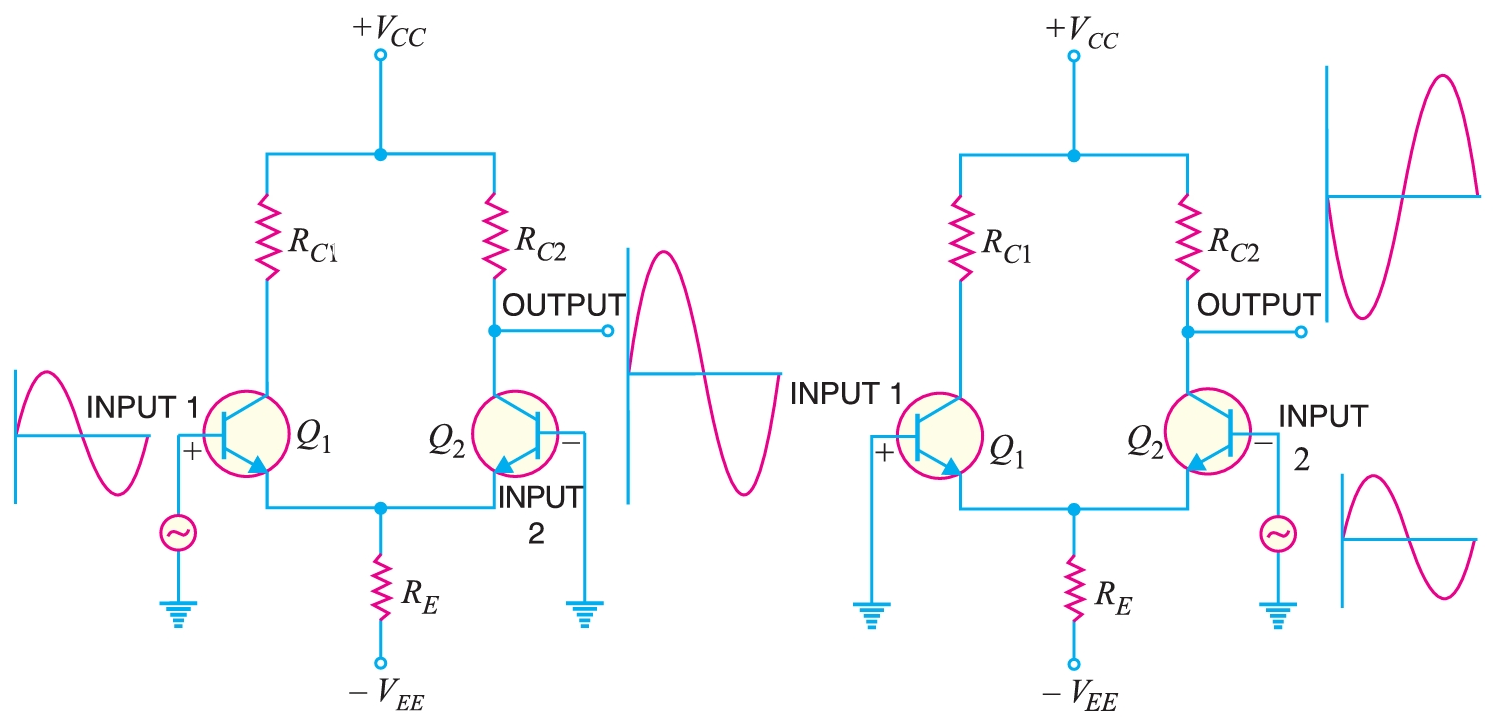
When a signal applied to the input of a differential amplifier produces no phase shift in the output, it is called a non-inverting input [See Fig. 5(i)]. In other words, for a noninverting input, the output signal is in phase with the input signal. When the signal applied to the input of differential amplifier produces 180° phase shift, it is called inverting input [See Fig. 5(ii)]. In other words, for inverting input, the output signal is 180° out of phase with the input signal. Since inverting the input provides a 180° phase shift, it is often identified with a \((–)\) sign. The noninverting input is then represented by a \((+)\) sign. The terms noninverting input and inverting input are meaningful when only one output terminal of the differential amplifier is available.
Common- and Differential-mode Signals
The importance of a differential amplifier lies in the fact that the outputs are proportional to the difference between the two input signals. Thus, the circuit can be used to amplify the difference between the two input signals or to amplify only one input signal by grounding the other. The input signals to a differential amplifier are defined as (i) Common-mode signals and (ii) Differential-mode signals.
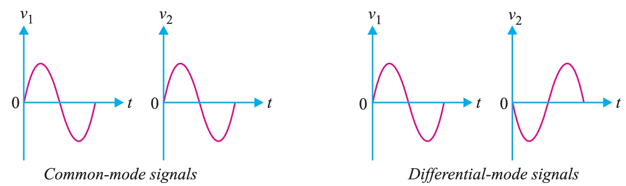
Common-mode signals
When the input signals to a differential amplifier are in phase and exactly equal in amplitude, they are called common-mode signals as shown in Fig. 6. The common-mode signals are rejected (not amplified) by the differential amplifier. A differential amplifier amplifies the difference between the two signals \((v_1 – v_2)\), and for common-mode signals, this difference is \(\text{zero}\).
For common-mode operations,
\[v_{1} = v_{2}\]
Differential-mode signals
When the input signals to a differential amplifier are 180° out of phase and exactly equal in amplitude, they are called differential-mode signals, as shown in Fig. 6. The differential-mode signals are amplified by the differential amplifier. It is because the difference in the signals is twice the value of each signal.
For differential-mode signals,
\[v_{1} = –v_{2}\]
Thus, a differential amplifier will amplify differential-mode signals while rejecting common-mode signals.
Voltage Gain
The voltage gain of a differential amplifier operating in differential mode is called differential-mode voltage gain and is denoted by \(A_{DM}\). The voltage gain of differential amplifier operating in common-mode is called common-mode voltage gain and is denoted by \(A_{CM}\). Ideally, a differential amplifier provides a very high differential-mode voltage gain and zero common-mode voltage gain. However, in practice, differential amplifiers exhibit a very small common-mode gain (usually much less than \(1\)) while providing a high differential voltage gain (usually several thousand). The higher the differential gain with respect to the common-mode gain, the better the performance of the differential amplifier in terms of rejection of common-mode signals.
Common-mode Rejection Ratio (CMRR)
A differential amplifier should have high differential voltage gain \((A_{DM})\) and very low common mode voltage gain \((A_{CM})\). The ratio \(A_{DM}/A_{CM}\) is called the common-mode rejection ratio (CMRR), i.e.,
\(\text{CMRR} = \frac{A_{DM}}{A_{CM}}\)
Very often, the \(\text{CMRR} \) is expressed in decibels \((\text{dB})\). The decibel measure for \(\text{CMRR}\) is given by;
\[\text{CMRR}_{\text{dB}} = 20\,\text{log}_{10}\, \frac{A_{DM}}{A_{CM}} = 20\,\text{log}_{10}\,\text{CMRR}\]
The following table shows the relation between the two measurements :
| \(\text{CMRR}\) | \(\text{CMRR}_{\text{dB}}\) |
|---|---|
| \(10\) | \(20\,\text{dB}\) |
| \(10^{3}\) | \(60\,\text{dB}\) |
| \(10^{5}\) | \(100\,\text{dB}\) |
| \(10^{7}\) | \(140\,\text{dB}\) |
The CMRR is the ability of a differential amplifier to reject the common-mode signals. The larger the CMRR, the better the differential amplifier is at eliminating common-mode signals. The differential amplifier in Fig. 7 has a differential voltage gain of 1500 (i.e., \(A_{DM} = 1500\)) and a common-mode gain of \(0.01\) (i.e., \(A_{CM} = 0.01\)).
\[ \therefore \text{CMRR} = \frac{1500}{0.01} = 150000\]
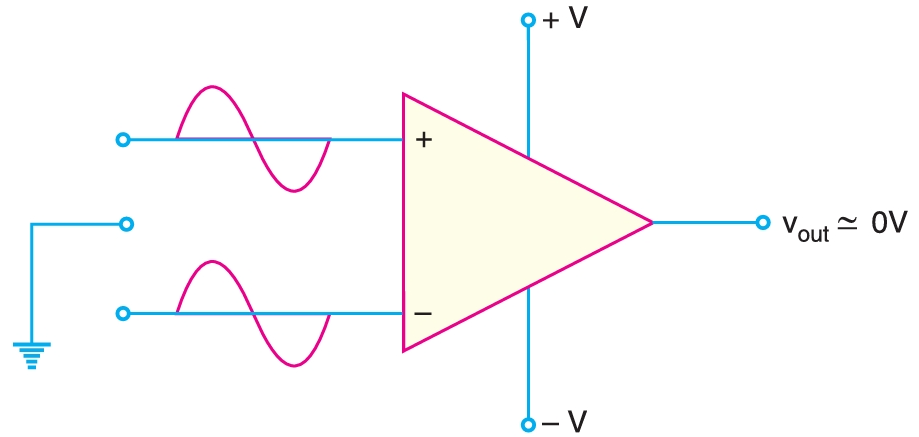
This means that the output produced by a difference between the inputs would be \(150000\) times as great as the output produced by a common-mode signal. The ability of the differential amplifier to reject common-mode signals is one of its main advantages. Common-mode signals are usually undesired signals caused by external interference. The high CMRR indicates the ability of differential amplifier to reject unwanted signals.
Fig. 8 shows how a differential amplifier (DA) rejects hum and static voltages induced into its input leads.
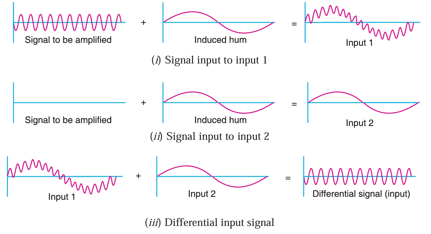
In Fig. 8, the signal is applied to input 1 of the differential amplifier. However, a low-frequency hum voltage is also induced into the lead wire. This hum is produced due to the building and collapsing magnetic field generated by an adjacent conductor carrying a \(50 \,\text{Hz}\) current. The resultant waveform is shown in Fig. 8(i). If this waveform is amplified by a conventional amplifier, the \(\text{50 \,\text{Hz}}\) hum in the output will be stronger than the desired signal.
However, a differential amplifier also has a second input (input \(2\)). Therefore, the lead of the second input has the same phase \(50 \,\text{Hz}\) hum induced into it. This is the only voltage (i.e., hum) applied to the input \(2\).
The hum components of the two inputs form a common-mode signal, which is largely rejected by the differential amplifier. If the input hum signals are equal at the input, then the differential input to the differential amplifier will be devoid of hum. Therefore, the amplified differential amplifier output will be free of hum.
This is the ideal case, i.e., \(A_{CM} = 0\). Even in a practical case, the value of \(A_{CM}\) is less than \(1\), while \(A_{DM}\) is over \(200\). This means that the desired signal would be over \(200\) times larger than the hum at the output terminal.
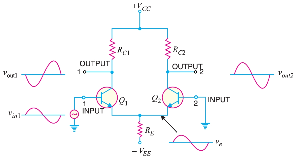
A differential amplifier is normally operated as double-ended input and single-ended output differential amplifier (DA). In other words, there are two input signals and one output signal.
When the input signal \(v_{1}\) (input \(1\)) is applied, the output signal is in phase with it, i.e., there is no phase shift. For this reason, the input signal \(v_{1}\) is called the non-inverting input.
When the input signal \(v_{2}\) (input \(2\)) is applied, the output signal is 180° out of phase with the input signal. For this reason, the input signal \(v_{2}\) is called the inverting input. The differential amplifier amplifies the difference between the two input voltages. The difference between the input voltages is
\[v_{\text{in}} = {v_1} – {v_2}\]
where \(v_{1}\) is the voltage applied to the noninverting input, \(v_{2}\) is the voltage applied to the inverting input, and \(v_{\text{in}}\) is the difference voltage that will be amplified. The differential amplifier is amplifying the difference between the input terminal voltages.
A.C. Analysis
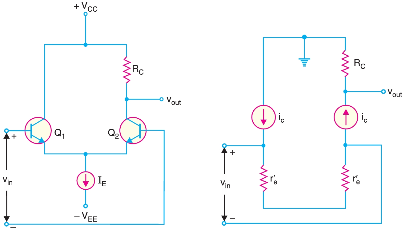
A differential amplifier (DA) has a noninverting input and an inverting input. Fig. 9 shows the differential amplifier (DA) used in IC OP-amps. The circuit has a double-ended input and a single-ended output.
The differential amplifier circuit in Fig. 9, responds to the difference between the voltages at the two input terminals. In other words, differential amplifier responds to \(v_{\text{in}} = {v_1} – {v_2}\). Therefore, the circuit shown in Fig. 9a can be drawn as shown in Fig. 9b.
Ideally (i.e., \(V_{BE}\) is negligible), the tail current \(I_{E}\) in Fig. 9a is \(I_{E} = V_{EE}/R_{E}\). Once the \(V_{EE}\) and \(R_{E}\) values are set, the tail current remains constant. Therefore, to simplify a.c. In analysis, we can replace the tail current with a current source \((I_{E})\), as shown in Fig. 10. This will simplify the a.c. analysis of the circuit with almost no loss of accuracy.
A.C. Equivalent Circuit.
The a.c. equivalent circuit of a differential amplifier by applying the usual rules, namely, to short all the capacitors, and reduce all the d.c. sources to zero. Since a differential amplifier has no capacitors, the d.c. sources are reduced to zero. Reducing a voltage source to zero is equivalent to replacing it with a short. Reducing a current source to zero is equivalent to opening it. In Fig. 10a, this means grounding the \(V_{CC}\) and \(V_{EE}\) points and opening the current source.
Applying these conditions to Fig. 10a, we get the a.c. equivalent circuit of the differential amplifier shown in Fig. 10b.
Voltage gain.
Fig. 10b shows the a.c. equivalent circuit of a differential amplifier. \(r_{e}\) \((= 25 \,\text{mV}/I_{E})\) is the a.c. emitter resistance. Since the two \(r_{e}\) are in series, the same a.c. The emitter current exists in both transistors. The a.c. emitter current is given by;
\[i_{e} = \frac{v_{\text{in}}}{2r_{e}}\]
The a.c. collector current is approximately equal to the a.c. emitter current, i.e., \(i_{c} \approx i_{e}\).
Output Voltage, \(v_{\text{out}}\),
\[v_{\text{out}} = i_{c}R_{C} \]
\[v_{\text{out}} = \frac{v_{\text{in}}}{2r_{e}}\,R_{C}\]
Voltage gain, \(A\),
\[A = \frac{v_{\text{out}}}{v_{\text{in}}} = \frac{R_{C}}{2r_{e}}\]
This gain of differential amplifier is referred to as differential-mode voltage gain and is usually denoted by \(A_{DM}\).
Input Impedance
The a.c. emitter current is given by;
\[i_{e} = \frac{v_{\text{in}}}{2r_{e}} = \beta\, i_{b}\]
Now \(i_{b}\) is the a.c. input current to the differential amplifier. Therefore, \(v_{\text{in}}/i_{b}\) is the input impedance.
\[\therefore \quad \frac{v_{\text{in}}}{i_{b}} = 2\,\beta\,r_{e}\]
or, Input impedance,
\[Z_{i} = 2\,\beta\,r_{e}\]
Common-mode Voltage Gain
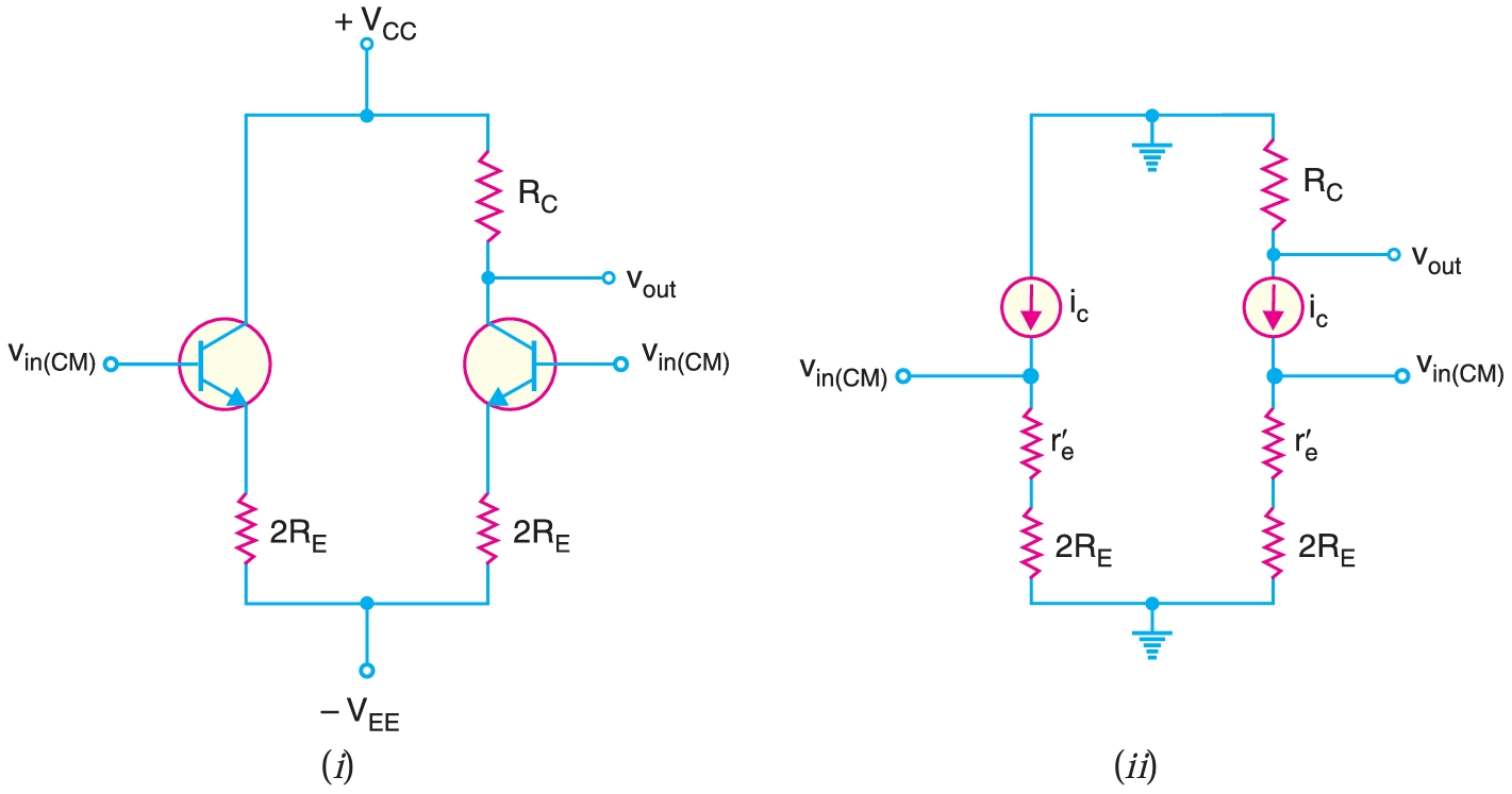
The common-mode signals have equal amplitudes and the same phase. Fig. 11a shows the common-mode operation of a differential amplifier (DA). The same input voltage, \(v_{in(CM)}\), is being applied to each base. Ideally, there is no a.c. output voltage with a common-mode input signal. It is because a differential amplifier is designed to respond to the difference between two input signals. If the inputs are identical, the differential amplifier output is zero. In practice, the two halves of the differential amplifier are never completely balanced, and there is a very small a.c. output voltage for the common-mode signal.
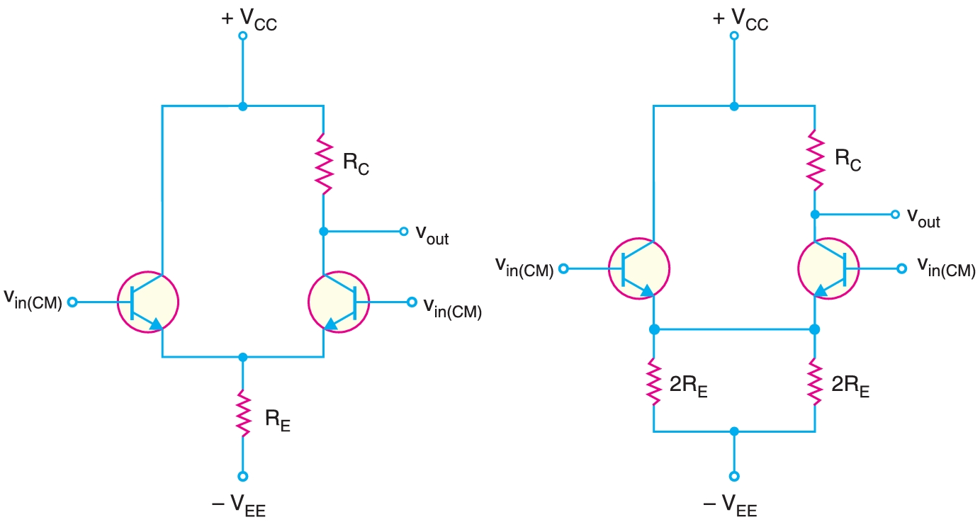
The circuit shown in Fig. 11a can be redrawn as shown in Fig. 11b. In this equivalent circuit, the two parallel resistances of \(2\, R_{E}\) produce an equivalent resistance of \(R_{E}\). Therefore, this equivalent circuit will not affect the output voltage. Assuming identical transistors, the two emitter currents will be equal and produce the same voltage across emitter resistors. Therefore, there is no current through the wire between the emitters. We can remove this wire, and the circuit becomes as shown in Fig. 12.
To get the a.c. equivalent circuit, we can reduce both supply voltages to zero, i.e., we ground each supply point. Replacing the transistors with their a.c. equivalent circuits, the a.c. equivalent circuit of a differential amplifier for common-mode operation as shown in Fig. 16
Common-mode voltage gain, \(A_{CM}\)
\[A_{CM} = \frac{v_{\text{out}}} {v_{\text{in CM}}} = \frac{R_C} {r_{e}+2\,R_{E}}\]
where \(r_{e}\) is a.c. emitter resistance \(= 26 \,\text{mV}/\text{d.c. emitter current}\). In most cases, \(r_{e}\) is very small as compared to \(R_{E}\) and hence, \(r_{e}\) is dropped from the formula.
\[\therefore A_{CM} = \frac{R_{C}}{2\,R_{E}} \]
The common-mode voltage gain \((A_{CM})\) is very small.