Applications of OP-Amps
The operational amplifiers have many practical applications. The OP-amp can be connected in a large number of circuits to provide various operating characteristics.
Inverting Amplifier
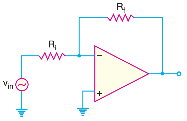
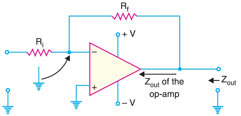
An OP amplifier can be operated as an inverting amplifier as shown in Fig. 1. An input signal \(v_{\text{in}}\) is applied through input resistor \(R_{\text{i}}\) to the minus input (inverting input). The output is fed back to the same minus input through feedback resistor \(R_{\text{f}}\). The plus input (noninverting input) is grounded. Note that the resistor \(R_{\text{f}}\) provides the negative feedback. Since the input signal is applied to the inverting input \((–)\), the output will be inverted (i.e. \(180°\) out of phase) as compared to the input. Hence the name inverting amplifier.
Voltage Gain
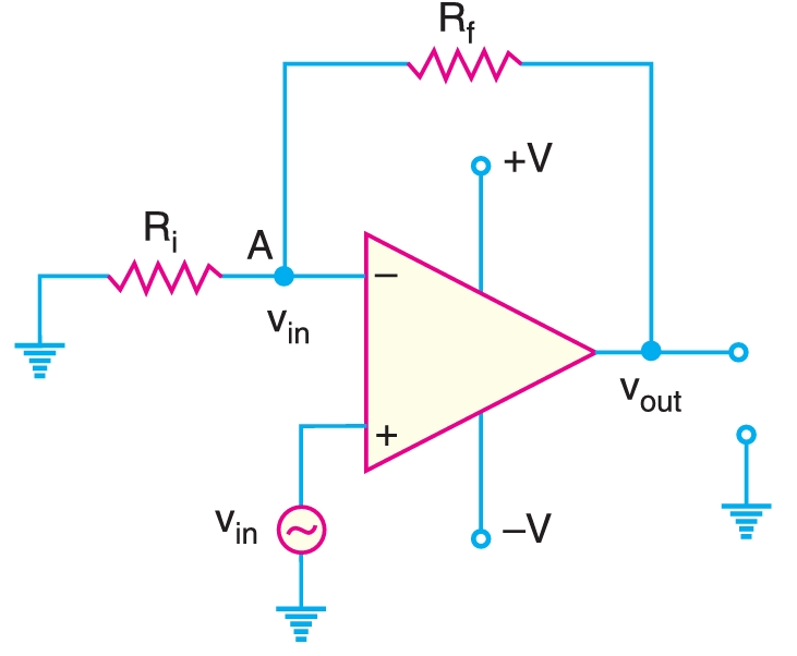
An OP-amp has an infinite input impedance or there is zero current at the inverting input. If there is zero current through the input impedance, then there must be no voltage drop between the inverting and non inverting inputs. This means that voltage at the inverting input \((–)\) is zero \((point \,\text{A})\) because the other input \((+)\) is grounded. The \(0\,\text{V}\) at the inverting input terminal \((point \,\text{A})\) is referred to as virtual ground. This condition is illustrated in Fig. 2.
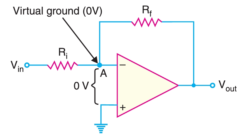
The point \(A\) is said to be at virtual ground because it is at \(0\,\text{V}\) but is not physically connected to the ground (i.e. \(V_{A} = 0\,\text{V}\)). Referring to Fig. 3, the current \(I_{1}\) to the inverting input is zero. Therefore, current \(I_{\text{in}}\) flowing through \(R_{\text{i}}\) entirely flows through feedback resistor \(R_{\text{f}}\). In other words,
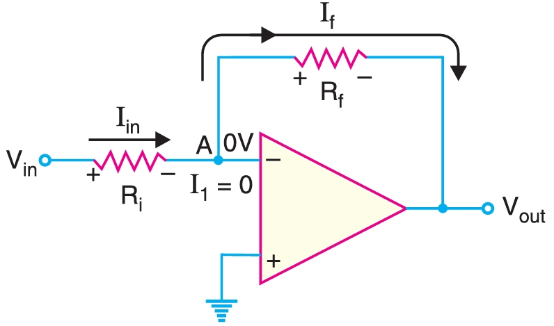
\[I_{f} = I_{\text{in}}\]
Now,
\[I_{\text{in}} = \frac{\text{Voltage across }R_{\text{i}}}{R_{\text{i}}}\]
\[I_{\text{in}} = \frac{V_{\text{in}} - V_{A}}{R_{\text{i}}} = \frac{V_{\text{in}} - 0}{R_{\text{i}}} = \frac{V_{\text{in}}}{R_{\text{i}}}\]
and
\[I_{\text{f}} = \frac{\text{Voltage across }R_{\text{f}}}{R_{\text{f}}}\]
\[I_{\text{f}} = \frac{V_{A}- V_{\text{out}}}{R_{\text{f}}} = \frac{0-V_{\text{out}}}{R_{\text{f}}} = \frac{-V_{\text{out}}}{R_{\text{f}}}\] \[\frac{-V_{\text{out}}}{R_{\text{f}}} = \frac{V_{\text{in}}}{R_{\text{i}}} \quad \because I_{f} = I_{\text{in}} \]
\[\therefore \quad \text{Voltage gain, } A_{CL} = \frac{-V_{\text{out}}}{V_{\text{in}}} = -\frac{R_{\text{f}}}{R_{\text{i}}}\]
The negative sign indicates that output signal is inverted as compared to the input signal. The closed-loop voltage gain \((A_{CL})\) of an inverting amplifier is the ratio of the feedback resistance \(R_{\text{f}}\) to the input resistance \(R_{\text{i}}\). The closed-loop voltage gain is independent of the internal open-loop voltage gain of OP-amp. Thus the negative feedback stabilizes the voltage gain. The inverting amplifier can be designed for unity gain by keeping \(R_{\text{f}} = R_{\text{i}}\), the voltage gain, \(A_{CL} = –1\). Therefore, the circuit provides a unity voltage gain with \(180°\) phase inversion. If \(R_{\text{f}}\) is some multiple of \(R_{\text{i}}\), the amplifier gain is constant. For example, if \(R_{\text{f}} = 10 \,R_{\text{i}}\), then \(A_{CL} = -10\) and the circuit provides a voltage gain of exactly \(10\) along with a \(180°\) phase inversion from the input signal. The precise selection of resistor values for \(R_{\text{f}}\) and \(R_{\text{i}}\), we can obtain a wide range of voltage gains. Thus the inverting amplifier provides constant voltage gain.
Input Impedance
While an OP-amp has an extremely high input impedance, the inverting amplifier does not. The reason for this can be seen by referring back to Fig. 3. The voltage source “sees” an input resistance \((R_{\text{i}})\) that is going to virtual ground. Thus the input impedance for the inverting amplifier is
\[Z_{\text{i}} = R_{\text{i}} \]
The value of \(R_{\text{i}}\) will always be much less than the input impedance of the OP amp. Therefore, the overall input impedance of an inverting amplifier will also be much lower than the OP-amp input impedance.
Output impedance
Fig. 4 shows the inverting amplifier circuit. The output impedance of the inverting amplifier is the parallel combination of \(R_{\text{f}}\) and the output impedance of OP-amp itself. The presence of the negative feedback circuit reduces the output impedance of the amplifier to a value that is less than the output impedance of OP-amp.
Non-inverting Amplifier
There are times when we wish to have an output signal of the same polarity as the input signal. In this case, the OP-amp is connected as noninverting amplifier as shown in Fig. 5. The input signal is applied to the noninverting input \((+)\). The output is applied back to the input through the feedback circuit formed by feedback resistor \(R_{\text{f}}\) and input resistance \(R_{\text{i}}\). Note that resistors \(R_{\text{f}}\) and \(R_{\text{i}}\) form a voltage divide at the inverting input \((–)\). This produces negative feedback in the circuit. Note that \(R_{\text{i}}\) is grounded. Since the input signal is applied to the noninverting input \((+)\), the output signal will be noninverted i.e., the output signal will be in phase with the input signal. Hence, the name non-inverting amplifier.
Voltage gain
If we assume that we are not at saturation, the potential at point \(\,\text{A}\) is the same as \(V_{\text{in}}\). Since the input impedance of OP-amp is very high, all of the current that flows through \(R_{\text{f}}\) also flows through \(R_{\text{i}}\).
\[\text{Voltage across } R_{\text{i}} = v_{{in}} – 0\]
\[\text{Voltage across } R_{\text{f}} = v_{\text{out}} – v_{\text{in}}\]
Now
\[\text{Current through } R_{\text{i}} = \text{Current through } R_{\text{f}} \]
\[\text{or} \quad \frac{v_{{in}} – 0}{R_{\text{i}}} = \frac{v_{\text{out}} – v_{\text{in}}}{R_{\text{f}}}\]
\[\text{or} \quad v_{\text{in}}R_{\text{f}} = v_{\text{out}}R_{\text{i}} - v_{\text{in}}R_{\text{i}}\]
\[\text{or} \quad v_{\text{in}}(R_{\text{f}}+R_{\text{i}}) = v_{\text{out}}R_{\text{i}}\]
\[\text{or} \quad \frac{v_{\text{out}}}{v_{\text{in}}} = \frac{R_{\text{f}}+R_{\text{i}}}{R_{\text{i}}} = 1+ \frac{R_{\text{f}}}{R_{\text{i}}}\]
\[\therefore \text{Closed-loop voltage gain, } A_{CL} = \frac{v_{\text{out}}}{v_{\text{in}}} = 1 + \frac{R_{\text{f}}}{R_{\text{i}}} \]
Hence, the voltage gain of noninverting amplifier also depends upon the values of \(R_{\text{f}}\) and \(R_{\text{i}}\). The voltage gain of a non inverting amplifier can be made equal to or greater than \(1\). The voltage gain of a non-inverting amplifier will always be greater than the gain of an equivalent inverting amplifier by a value of \(1\). If an inverting amplifier has a gain of \(150\), the equivalent noninverting amplifier will have a gain of \(151\). The voltage gain is positive because output signal is in phase with the input signal.
Voltage Follower
The voltage follower arrangement is a special case of noninverting amplifier where all of the output voltage is fed back to the inverting input as shown in Fig. 6. The \(R_{\text{i}}\) and \(R_{\text{f}}\) are removed from the non-inverting amplifier and short the output of the amplifier to the inverting input. The voltage gain for the voltage follower is calculated as under:
\[A_{CL} = 1+\frac{R_{\text{f}}}{R_{\text{i}}} = 1+\frac{0}{R_{\text{i}}} = 1 \quad (\because R_{\text{i}} = 0\,\Omega) \]
Thus the closed-loop voltage gain of the voltage follower is \(1\). The most important features of the voltage follower configuration are its very high input impedance and its very low output impedance. These features make it a nearly ideal buffer amplifier to be connected between high-impedance sources and low-impedance loads.
Summing Amplifiers
A summing amplifier is an inverted OP-amp that can accept two or more inputs. The output voltage of a summing amplifier is proportional to the negative of the algebraic sum of its input voltages. Hence the name summing amplifier. Fig. 7 shows a three-input summing amplifier but any number of inputs can be used. Three voltages \(V_{1}\), \(V_{2}\) and \(V_{3}\) are applied to the inputs and produce currents \(I_{1}\), \(I_{2}\) and \(I_{3}\). Using the concepts of infinite impedance and virtual ground, the inverting input of the OP-amp is at virtual ground \((0\,\text{V})\) and there is no current to the input. This means that the three input currents \(I_{1}\), \(I_{2}\) and \(I_{3}\) combine at the summing point \(A\) and form the total current \((I_{f})\) which goes through \(R_{\text{f}}\)
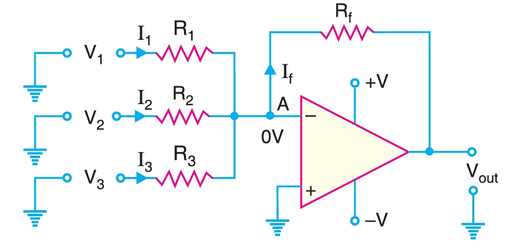
\[I_{f} = I_{1} + I_{2} + I_{3} \]
When all the three inputs are applied, the output voltage \((V_{\text{out}})\) is
\[V_{\text{out}} =– I_{f} R_{\text{f}} = – R_{\text{f}} (I_{1} + I_{2} + I_{3})\]
\[V_{\text{out}}=– R_{\text{f}}\left(\frac{V_{1}}{R_{1}} + \frac{V_{2}}{R_{2}} +\frac{V_{3}}{R_{3}} \right)\]
\[\therefore \quad V_{\text{out}} =– R_{\text{f}}\left(\frac{V_{1}}{R_{1}} + \frac{V_{2}}{R_{2}} +\frac{V_{3}}{R_{3}} \right)\]
If \(R_{1} = R_{2} = R_{3} = R\), then, we have,
\[V_{\text{out}} = -\frac{R_{\text{f}}}{R} (V_{1} + V_{2} + V_{3})\]
Thus the output voltage is proportional to the algebraic sum of the input voltages (of course neglecting negative sign). An interesting case results when the gain of the amplifier is unity. In that case, \(R_{\text{f}} = R_{1} = R_{2} = R_{3}\) and output voltage is
\[V_{\text{out}} =– (V_1 + V_2 + V_3)\]
Thus, when the gain of summing amplifier is unity, the output voltage is the algebraic sum of the input voltages.
When \(R_{\text{f}}\) is larger than the input resistors, the OP-amp has a gain of \(R_{\text{f}}/R\) where \(R\) is the value of each input resistor. The general expression for the output voltage is
\[V_{\text{out}} = -\frac{R_{\text{f}}}{R} (V_{1} + V_{2} + V_{3})\]
The output voltage is the sum of input voltages multiplied by a constant determined by the ratio \(R_{\text{f}} /R\).
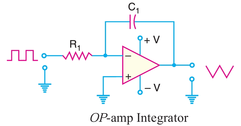
OP-Amp Integrator
A circuit that performs the mathematical integration of input signal is called an integrator. The output of an integrator is proportional to the area of the input waveform over a period of time.
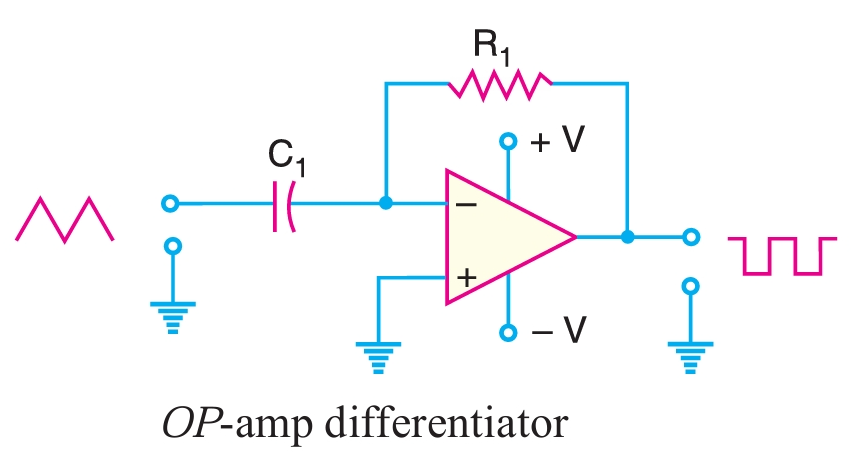
A circuit that performs the mathematical differentiation of input signal is called a differentiator. The output of a differentiator is proportional to the rate of change of its input signal.
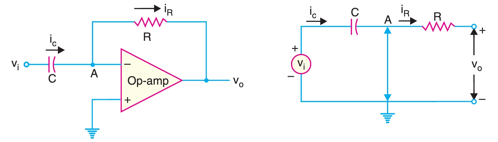
An integrator is a circuit that performs integration of the input signal. The integrator produces a ramp output voltage (i.e. a linearly increasing or decreasing voltage) up on a square wave input. Fig. 8 shows the circuit of an OP-amp integrator. It consists of an OP-amp, input resistor \(R\) and feedback capacitor \(C\). The feedback component is a capacitor instead of a resistor. When a signal is applied to the input of this circuit, the output-signal waveform will be the integration of input-signal waveform.
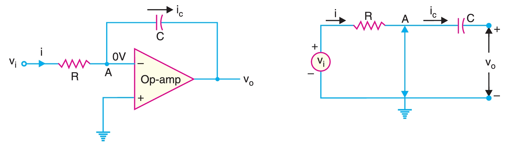
Circuit Analysis
The virtual-ground equivalent circuit of operational integrator will be as shown in Fig. 10. Because of virtual ground and infinite impedance of the OP-amp, all of the input current \(i\) flows through the capacitor, i.e., \[i = i_c\] Now
\[i = \frac{v_{\text{i}}-0}{R} = \frac{v_{\text{i}}}{R}\]
Also voltage across capacitor is
\[v_{c} = 0 – v_{o} = – v_{o}\]
\[\therefore i_{c} = \frac{C\,dv_{c}} {dt} =− \frac{C\, dv_{o}} {dt}\]
\[\text{or} \quad \frac{v_{\text{i}}-0}{R} = − {C dv_{o}} {dt} \]
\[\text{or} \quad − \frac{dv_{o}}{dt} = \frac{v_{\text{i}}-0}{RC}\]
To find the output voltage, we integrate both sides to get,
\[v_{o} = − \frac{1}{RC} \int_{0}^{t} v_{\text{i}}\, dt\]
The expression shows that the output is the integral of the input with an inversion and scale multiplier of \(1/RC\).
Output voltage
When a fixed voltage is applied to the input of an integrator, the output voltage grows over a period of time, providing a ramp voltage. The output voltage ramp (for a fixed input voltage) is opposite in polarity to the input voltage and is multiplied by the factor \(1/RC\).
Critical Frequency
The integrator shown in Fig. 10 has no feedback at \(0 \,\text{Hz}\). This is a serious disadvantage in low-frequency applications. By connecting a feedback resistor \(R_{\text{f}}\) in parallel with the capacitor, precise closed-loop voltage gain is possible. The circuit shown in Fig. 11 is an integrator with a feedback resistor \(R_{\text{f}}\) to provide increased stability. All integrators have a critical frequency \(f_{c}\) below which they do not perform proper integration. When the input frequency is less than \(f_{c}\), the circuit behaves like a simple inverting amplifier and no integration occurs.
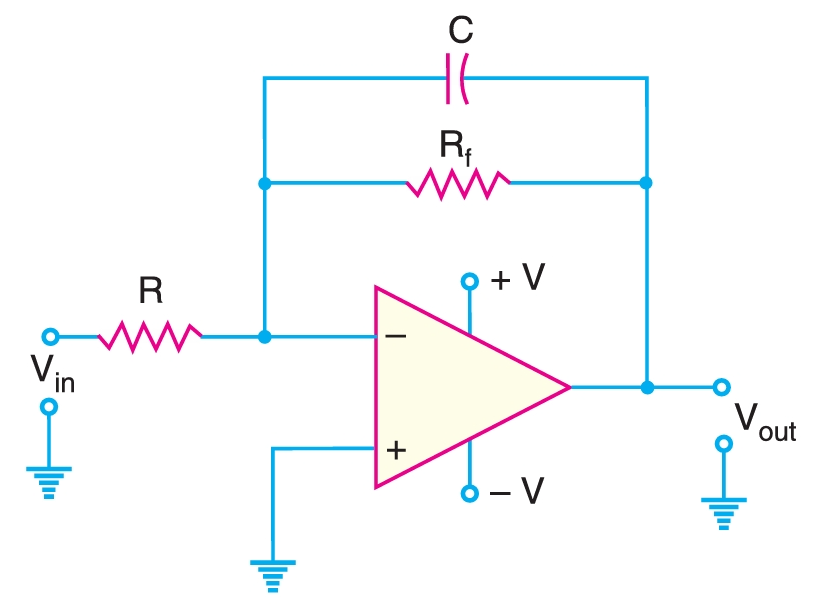
The expression to calculate the critical frequency of an integrator is:
\[f_{c} = \frac{1}{2\pi R_{\text{f}}C} \]
OP-Amp Differentiator
A differentiator is a circuit that performs differentiation of the input signal. A differentiator produces an output voltage that is proportional to the rate of change of the input voltage. Its important application is to produce a rectangular output from a ramp input. Fig. 12 shows the circuit of OP-amp differentiator. It consists of an OP-amp, an input capacitor \(C\) and feedback resistor \(R\). The placement of the capacitor and resistor are swiped in differentiator when compared with the integrator. The capacitor is the input element. Since point \(A\) in Fig. 12 is at virtual ground, the virtual-ground equivalent circuit of the operational differentiator is as shown in Fig. 12. Because of virtual ground and infinite impedance of OP-amp, all the input current \(i_{c}\) flows through the feedback resistor \(R\), i.e.,
\[i_{c} = i_{R} \]
\[\therefore i_{R} = \frac{0 − v_{o}}{R}=\frac{-v_{o}}{R} \]
and
\[v_{c} = v_{\text{i}} \, – \, 0 = v_{\text{i}} \]
Also
\[i_{c} = \frac{Cdv_{c}}{dt} = \frac{Cdv_{\text{i}}}{dt}\]
\[\therefore − \frac{v_o}{R} = C \frac{dv_{\text{i}}} {dt} \quad (\because i_{R} = i_{c}) \]
\[\text{or} \quad v_{o} =– RC \frac{dv_i} {dt} \]
The expression for output voltage shows that output is the differentiation of the input with an inversion and scale multiplier of \(RC\). When the input voltage is constant, \(dv_{\text{i}}/dt\) is \(\text{zero}\) and the output voltage is \(\text{zero}\). The faster the input voltage changes, the larger the magnitude of the output voltage.
Comparators
A comparator may be used to compare one voltage to another voltage source. A comparator is an OP-amp circuit without negative feedback and takes advantage of very high open-loop voltage gain of OP-amp. A comparator has two input voltages (non-inverting and inverting) and one output voltage. A very small difference voltage between the two inputs drives the amplifier to saturation because of the high open-loop voltage gain of an OP-amp. This is the key point in the working of comparator.
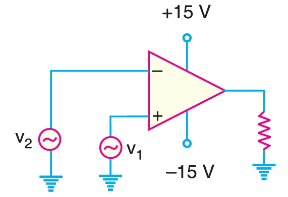
Fig. 13 illustrates the action of a comparator. The input voltages are \(v_{1}\) (signal) and \(v_{2}\) (reference voltage). When the differential input is positive, the circuit is driven to saturation and output goes to maximum positive value \((+V_{\text{sat}})\). Reverse happens when the differential input goes negative, i.e., the output is maximum negative \((–V_{\text{sat}})\). This circuit is called comparator because it compares \(v_1\) to \(v_2\) to produce a saturated positive or negative output voltage. The output voltage rapidly changes from \(-V_{\text{sat}}\) to \(+V_{\text{sat}}\) and vice-versa. A comparator circuit has two characteristics, namely, it uses no feedback so that the voltage gain is equal to the open-loop voltage gain \((A_{OL})\) of OP-amp and it is operated in a non-linear mode. These properties of a comparator permit it to perform many useful functions.
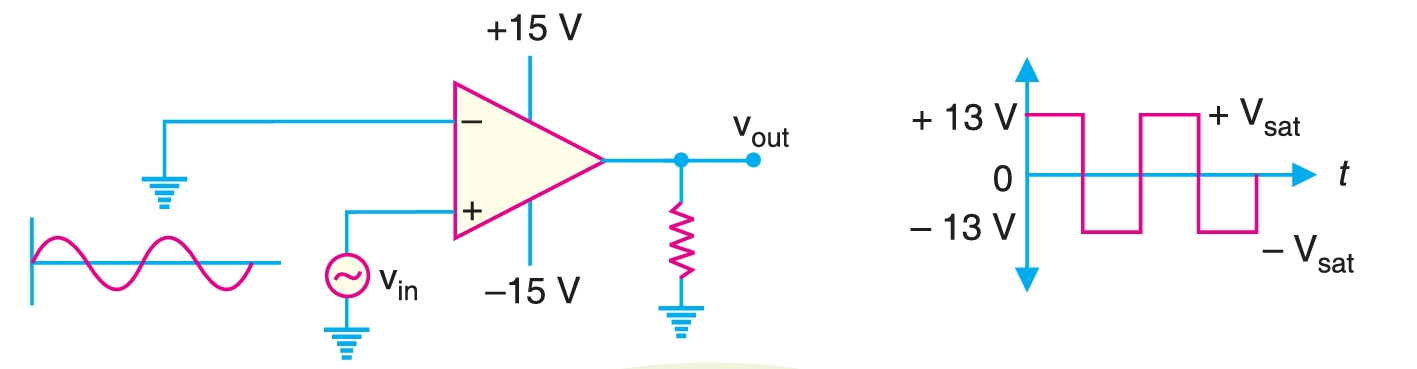
Square wave generator
A comparator can be used to produce a square wave output from a sine wave input. Fig. 14 shows the circuit of a comparator to produce square wave output. The inverting terminal \((–)\) is grounded and signal \((v_{\text{in}})\) is applied to the noninverting terminal \((+)\). Since the gain of a comparator is equal to \(A_{OL}\), virtually any difference voltage at the inputs will cause the output to go to one of the voltage extremes (\(+V_{\text{sat}}\) or \(–V_{\text{sat}}\)) and stay there until the voltage difference is removed. The polarity of the input difference voltage will determine to which extreme (\(+V_{\text{sat}}\) or \(–V_{\text{sat}}\)) the output of the comparator goes. When the input signal goes positive, the output jumps to about \(+V_{\text{sat}}\). When the input goes negative, the output jumps to about \(–V_{\text{sat}}\). The output changes rapidly from \(–V_{\text{sat}}\) to \(+ V_{\text{sat}}\) and vice-versa. This change is so rapid that we get a square wave output for a sine wave input.
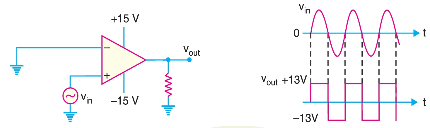
Zero-crossing detector
When one input of a comparator is connected to ground, it is known as zero-crossing detector because the output changes when the input crosses \(0 \,\text{V}\). The zero crossing circuit is shown in Fig. 15. The input and output waveforms are also shown. When the input signal is positive-going, the output is driven to positive maximum value (i.e. \(+V_{\text{sat}}\)). When the input crosses the zero axis and begins to go negative, the output is driven to negative maximum value (i.e. \(–V_{\text{sat}}\)). Every time the input crosses \(0 \,\text{V}\) going positive, the output jumps to \(+V_{\text{sat}}\). Similarly, every time the input crosses \(0 \,\text{V}\) going negative, the output jumps to \(–V_{\text{sat}}\). Since the change (\(+V_{\text{sat}}\) or \(–V_{\text{sat}}\)) occurs every time the input crosses \(0 \,\text{V}\), the zero crossing of the input signal can be detected and hence, the name zero-crossing detector.
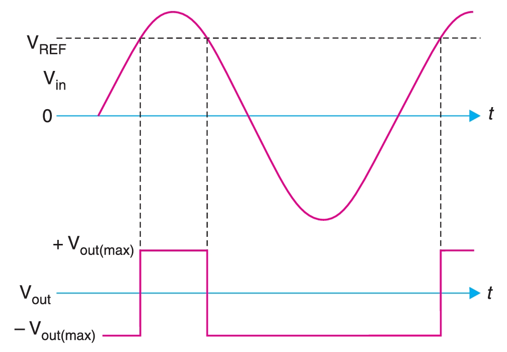
Level detector
When a comparator is used to compare a signal amplitude to a fixed d.c. level (reference voltage), the circuit is referred to as a level detector. The zero crossing detector circuit is modified to construct level detector. This can be done by connecting a fixed reference voltage \(V_{REF}\) to the inverting input. A practical arrangement is shown in Fig. 16 using a voltage divider to set the reference voltage as follows:
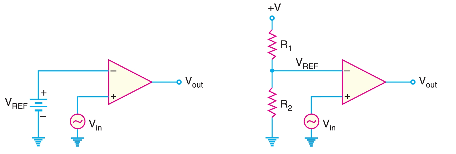
\[V_{\text{REF}} = \frac{R_2}{R_1+R_2} (+ \text{V})\]
where \(+\text{V}\) is the positive OP-amp d.c. supply voltage.
Consider the input signal \(v_{\text{in}}\) as a sine wave. When the input voltage is less than the reference voltage (i.e., \(v_{\text{in}} \lt V_{REF}\)), the output goes to maximum negative level. It remains here until \(v_{\text{in}}\) increases above \(V_{REF}\). When the input voltage exceeds the reference voltage (i.e. \(v_{\text{in}} \gt V_{REF}\)), the output goes to its maximum positive state. It remains here until \(v_{\text{in}}\) decreases below \(V_{REF}\). Fig. 17 shows the input/output waveforms. The circuit is used for non-zero level detection.