Flip-Flops:
Flip-flops are fundamental building blocks in digital circuits, serving as memory elements that store binary information. These bistable devices have a wide range of applications, from basic memory storage to more complex sequential logic circuits.
Types of Flip-Flops
- SR Flip-Flop (Set-Reset Flip-Flop): The SR flip-flop has two inputs: Set (S) and Reset (R). It can store one bit of information, typically representing 0 or 1. Depending on the inputs, it can be in one of four states: Set, Reset, Hold, or Indeterminate. The latter occurs when both inputs are active simultaneously.
- JK Flip-Flop: The JK flip-flop is an evolution of the SR flip-flop, addressing the indeterminate state issue. It features J (Jump) and K (Kill) inputs, which allow for toggling and complementing the output respectively. It has four possible states: Set, Reset, Toggle, and Hold.
- D Flip-Flop (Data Flip-Flop): The D flip-flop has a single input, Data (D), which directly controls the output state. Its simplicity makes it useful in applications where synchronous memory elements are required.
- T Flip-Flop (Toggle Flip-Flop): The T flip-flop takes a Toggle (T) input. When the T input is high, the output toggles, making it useful for frequency division and generating square waves.
SR Flip-Flops:
The S-R (Set-Reset) flip-flop is one of the simplest and most widely used. The S-R flip-flop consists of two inputs, the Set (S) and Reset (R) inputs, and two outputs, the Q and Q̅ outputs. The Q output represents the stored data bit, while Q̅ is its complement. The behavior of the S-R flip-flop is determined by its truth table, which outlines how it responds to various combinations of inputs.
Truth Table:
| S | R | Q(t) | Q̅(t) | Description |
|---|---|---|---|---|
| 0 | 0 | Q(t) | Q̅(t) | No change (hold state) |
| 0 | 1 | 0 | 1 | Reset |
| 1 | 0 | 1 | 0 | Set |
| 1 | 1 | ? | ? | Invalid state (ambiguous) |
In the truth table, "Q(t)" represents the current state of the Q output at time "t" and "Q̅(t)" is its complement. The invalid state occurs when both S and R are set to 1 simultaneously, leading to unpredictable behavior.
The S-R flip-flop operates based on the concept of cross-coupled NAND gates. When both S and R are 0, the flip-flop holds its state. When S is 1 and R is 0, the flip-flop is set (Q becomes 1, Q̅ becomes 0). Conversely, when S is 0 and R is 1, the flip-flop is reset (Q becomes 0, Q̅ becomes 1). When both S and R are 1, the flip-flop enters an ambiguous state, and this condition must be avoided.
NAND gates can be used to construct various logic gates and flip-flops. An SR flip-flop can be built using NAND gates, allowing for a deeper understanding of its internal workings.
SR Flip-Flop Construction
An SR flip-flop can be created using two NAND gates. The following is the implementation:
- Connect both S and R inputs to the respective inputs of the first NAND gate.
- Connect the output of the first NAND gate to both inputs of the second NAND gate.
- The output of the second NAND gate is Q̅, and its complement (Q) can be obtained by connecting Q̅ to an inverter.
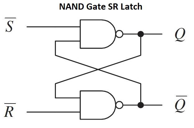
Truth Table Validation
Consider two NAND gates: NAND1 and NAND2. The inputs S and R are connected to the inputs of NAND1. The outputs of NAND1 and NAND2 are Q̅ and Q, respectively. The circuit's behavior aligns with the SR flip-flop truth table:
| S | R | NAND1 | NAND2 | Q(t+1) | Q̅(t+1) |
|---|---|---|---|---|---|
| 0 | 0 | 1 | 1 | Q(t) | Q̅(t) |
| 0 | 1 | 1 | 0 | 0 | 1 |
| 1 | 0 | 0 | 1 | 1 | 0 |
| 1 | 1 | 0 | 0 | 0 | 0 |
Limitation of SR Flip-Flop
SR flip-flops have some limitations. One of the main issues with the basic SR flip-flop is the possibility of entering the forbidden state (S=1, R=1). This state leads to unpredictable behavior and is usually avoided by introducing additional logic to ensure that the flip-flop transitions only occur as intended.
Multivibrators
Individual Sequential Logic circuits can be used to build more complex circuits such as ounters, Shift Registers, Latches or Memories etc, but for these types of circuits to operate in a Sequential way, they require the addition of a clock pulse or timing signal to cause them to change their state. Clock pulses are generally square shaped waves that are produced by a single pulse generator circuit such as a Multivibrator which oscillates between a HIGH and a LOW state and generally has an even 50% duty cycle, that is it has a 50% ON time and a 50% OFF time. Sequential logic circuits that use the clock signal for synchronization may also change their state on either the rising or falling edge, or both of the actual clock signal. There are basically three types of pulse generation circuits depending on the number of stable states,
- Astable - has NO stable states but switches continuously between two states this action produces a train of square wave pulses at a fixed frequency.
- Monostable - has only ONE stable state and if triggered externally, it returns back to its first stable state.
- Bistable - has TWO stable states that produces a single pulse either positive or negative in value.
IC 555 TIMER
The 555 timer IC was first introduced around 1971 by the Signetics Corporation as the SE555/NE555 and was called The IC Time Machine and was also the very first and only commercial timer IC available. It provided circuit designers with a relatively cheap, stable, and user-friendly integrated circuit for timer and multivibrator applications. These ICs come in two packages, either the round metal-can called the T package or the more familiar 8-pin DIP V package as shown in figure below. The IC comprises of 23 transistors, 2 diodes, and 16 resistors with built-in compensation for component tolerance and temperature drift.
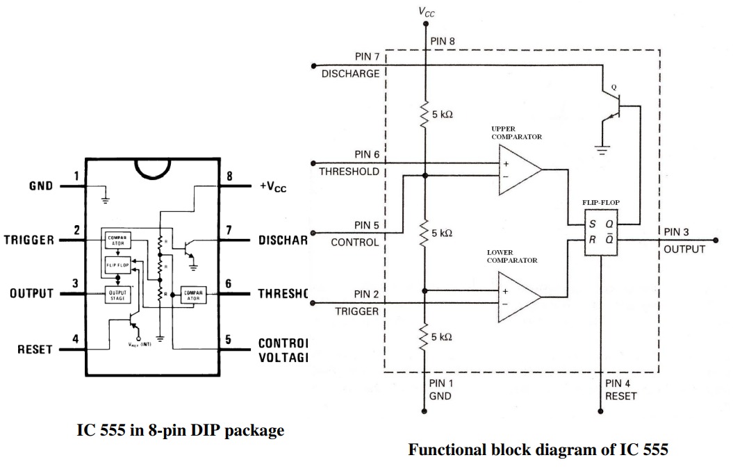
The pin connections are as follows:
- Ground.
- Trigger input.
- Output.
- Reset input.
- Control voltage.
- Threshold input.
- Discharge.
- \(+V_{CC}\) - \(+5\) to \(+15\) volts in normal use.
- Pin 1: Ground. All voltages are measured with respect to this terminal.
- Pin 2: Trigger. The output of the timer depends on the amplitude of the external trigger pulse applied to this pin. When a negative going pulse of amplitude greater than 1/3 \(V_{CC}\) is applied to this pin, the output of the timer high. The output remains high as long as the trigger terminal is held at a low voltage.
- Pin 3: Output. The output of the timer is measured here with respect to ground. There are two ways by which a load can be connected to the output terminal: either between pin 3 and ground or between pin3 and supply voltage \(+V_{CC}\). When the output is low the load current flows through the load connected between pin3 and \(+V_{CC}\) into the output terminal and is called sink current. The current through the grounded load is zero when the output is low. For this reason the load connected between pin 3 and \(+V_{CC}\) is called the normally on load (we will use this for our circuit) and that connected between pin 3 and ground is called normally off-load. On the other hand, when the output is high the current through the load connected between pin 3 and \(+V_{CC}\) is zero. The output terminal supplies current to the normally off load. This current is called source current. The maximum value of sink or source current is 200mA.
- Pin 4: Reset. The 555 timer can be reset (disabled) by applying a negative pulse to this pin. When the reset function is not in use, the reset terminal should be connected to \(+V_{CC}\) to avoid any possibility of false triggering.
- Pin 5: Control Voltage. An external voltage applied to this terminal changes the threshold as well as trigger voltage. Thus by imposing a voltage on this pin or by connecting a pot between this pin and ground, the pulse width of the output waveform can be varied. When not used, the control pin should be bypassed to ground with a \(0.01 ~\mu\text{F}\) Capacitor to prevent any noise problems.
- Pin 6: Threshold. When the voltage at this pin is greater than or equal to the threshold voltage 2/3 \(V_{CC}\), the output of the timer low.
- Pin 7: Discharge. This pin is connected internally to the collector of transistor Q. When the output is high Q is OFF and acts as an open circuit to external capacitor C connected across it. On the other hand, when the output is low, Q is saturated and acts as a short circuit, shorting out the external capacitor C to ground.
- Pin 8: \(+V_{CC}\). The supply voltage of +5V to + 18V is applied to this pin with respect to ground.
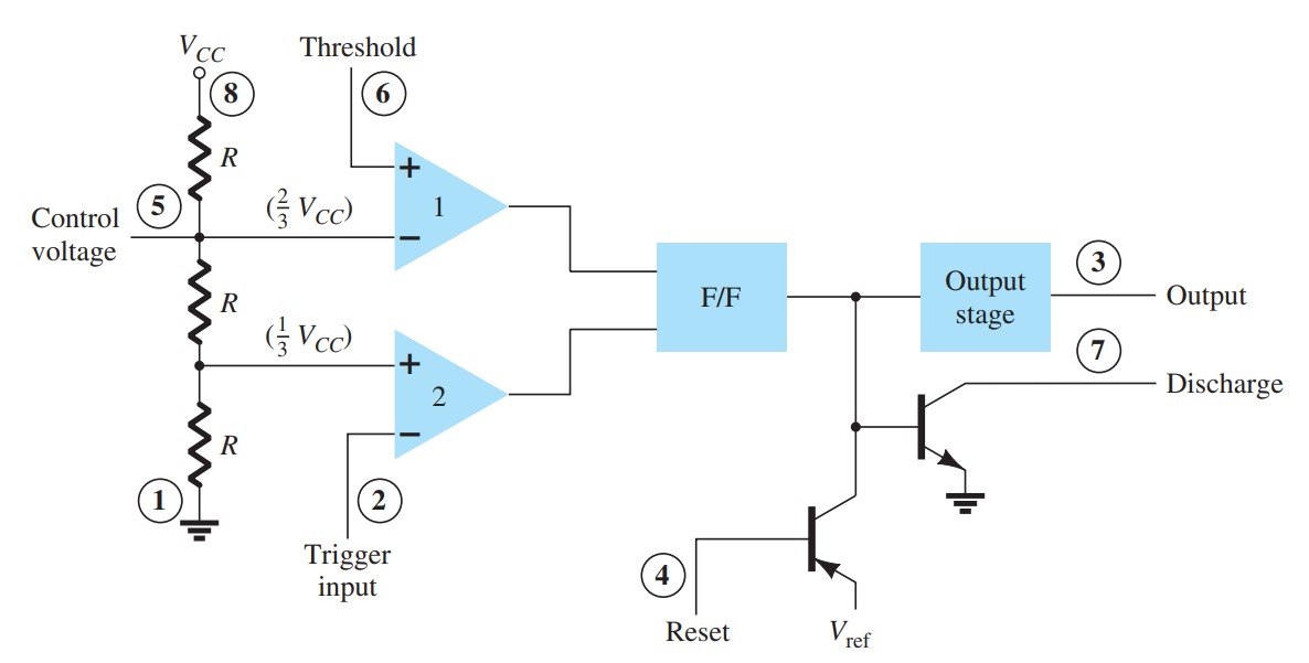
The IC is made of a combination of linear comparators and digital flip-flops as described in Fig. The entire circuit is usually housed in an eight-pin package as specified in Fig. A comparator is an OPAMP that compares an input voltage and indicates whether an input is higher or lower than a reference voltage by swinging into saturation in both the direction. A series connection of three resistors sets the reference voltage levels to the two comparators at \(2~ V_{CC}\gt 3\) and \(V_{CC}\gt 3\), the output of these comparators setting or resetting the flip-flop unit. The output of the flip-flop circuit is then brought out through an output amplifier stage. The flip-flop circuit also operates a transistor inside the IC, the transistor collector usually being driven low to discharge a timing capacitor.
The 555 can operate in either mono/bi-stable or astable mode, depending on the connections to and the arrangement of the external components. Thus, it can either produce a single pulse when triggered, or it can produce a continuous pulse train as long as it remains powered.
Astable Operation
One popular application of the 555 timer IC is as an astable multivibrator or clock circuit.
These circuits are not stable in any state and switch outputs after predetermined time periods. The result of this is that the output is a continuous square/rectangular wave with the properties depending on values of external resistors and capacitors. Thus, while designing these circuits following parameters need to be determined:
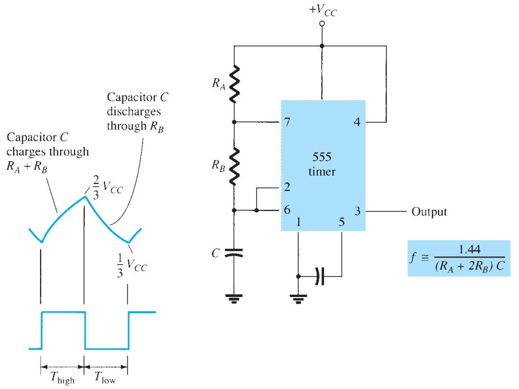
- Frequency (or the time period) of the wave.
- The duty cycle of the wave.
The time period of the pulse is defined as T and duration of the pulse (ON time) is \(\tau\). Duty cycle can be defined as the On time/Period that is, \(\tau/T\). a duty cycle of 50% will yield a square wave.
The following analysis of the operation of the 555 as an astable circuit includes details of the different parts of the unit and how the various inputs and outputs are used. Figure shows an astable circuit built using an external resistor and capacitor to set the timing interval of the output signal.
Capacitor C charges toward \(V_{CC}\) through external resistors \(R_A\) and \(R_B\). Refering to figure, we see that the capacitor voltage rises until it goes above \(2 V_{CC}\gt 3\). This voltage is the threshold voltage at pin 6, which drives comparator 1 to trigger the flip-flop so that the output at pin 3 goes low. In addition, the discharge transistor is driven on, causing the output at pin 7 to discharge the capacitor through resistor \(R_B\). The capacitor voltage then decreases until it drops below the trigger level ( \(V_{CC}\gt 3\)). The flip-flop is triggered so that the output goes back high and the discharge transistor is turned off, so that the capacitor can again charge through resistors \(R_A\) and \(R_B\) toward \(V_{CC}\).
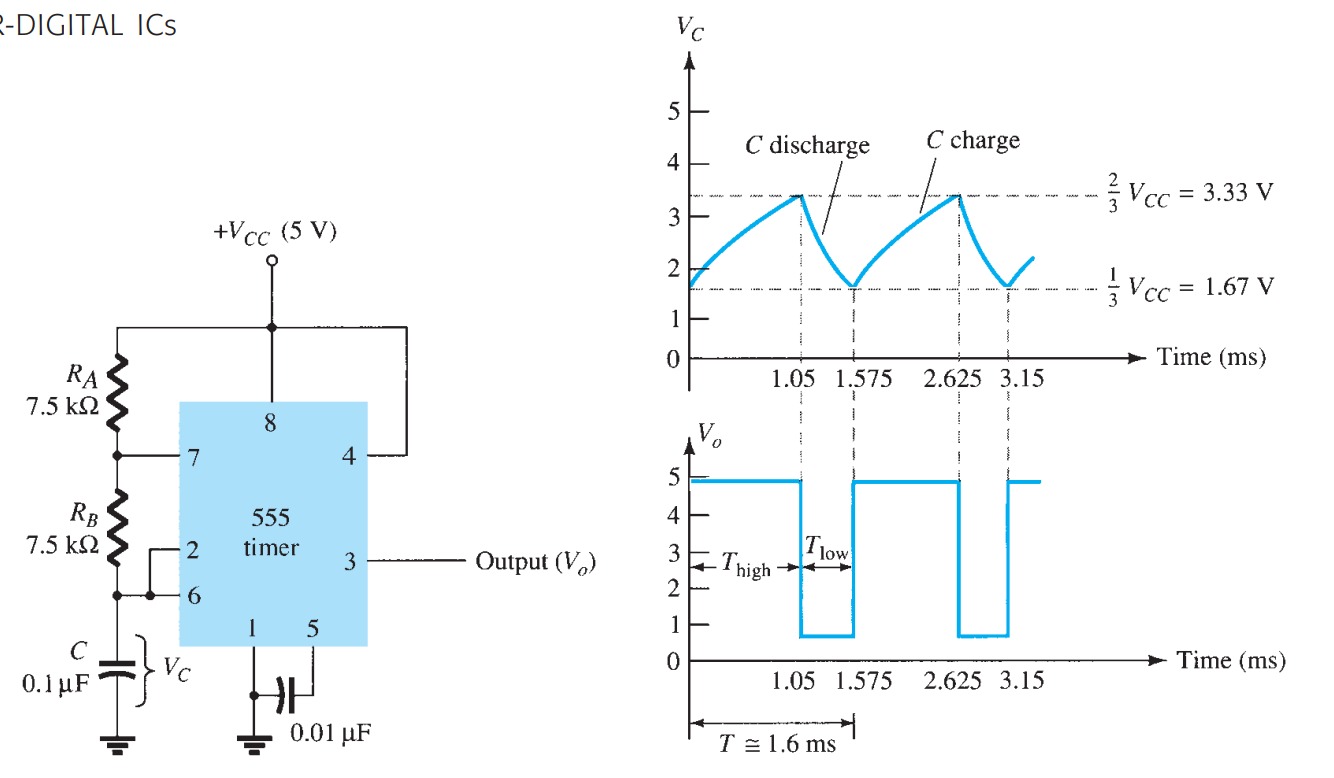
Figure a shows the capacitor and output waveforms resulting from the astable circuit. Calculation of the time intervals during which the output is high and low can be made using the relations
\[T_{\text{high}} = 0.693\,(R_{A} + R_{B})C \]
The coefficient 0.693 in the expression for \(T_{high}\) in a 555 astable multivibrator comes directly from the mathematics of capacitor charging and discharging in an RC circuit.
The capacitor in the astable circuit charges through resistors \(R_{\text{charging}} = R_A + R_B\) and discharges through \(R_{\text{discharging}} = R_B\). The voltage across a charging capacitor follows the exponential law while charging or discharging:
\[ V(t) = V_{CC} \cdot \left(1 - e^{-t/(RC)}\right) + V_{initial} \cdot e^{-t/(RC)} \]
In the 555 timer, the capacitor charges until it reaches 2/3 of \(V_{CC}\) and discharges until it falls to 1/3 of \(V_{CC}\). The time taken to go from 1/3 to 2/3 of \(V_{CC}\) is derived by solving the exponential equation.
The initial condition of voltage from the beginning of charging the capacitor is \(V_{initial} = \tfrac{1}{3} V_{CC}\), and the final voltage before discharging is \(V(t) = \tfrac{2}{3} V_{CC}\). i.e., At \(t=0\), \(V(0) = \tfrac{1}{3} V_{CC}\), hence, \(V_{initial} = \tfrac{1}{3} V_{CC}\) and the maximum voltage charge by the capacitor at the time \(t\) is when \(V(t) = \tfrac{2}{3} V_{CC} \).
Substituting the values in the general capacitance equation, we get,
\[ \tfrac{2}{3} V_{CC} = V_{CC} \cdot \left(1 - e^{-t/(RC)}\right) + \tfrac{1}{3} V_{CC} \cdot e^{-t/(RC)} \]
Divide through by \(V_{CC}\):
\[ \tfrac{2}{3} = 1 - e^{-t/(RC)} + \tfrac{1}{3} e^{-t/(RC)} \]
So,
\[ \tfrac{2}{3} = 1 - \tfrac{2}{3} e^{-t/(RC)} \]
Rearranging:
\[ \tfrac{2}{3} e^{-t/(RC)} = 1 - \tfrac{2}{3} = \tfrac{1}{3} \]
and solving for the exponential term, we get, \[ e^{-t/(RC)} = \tfrac{1}{2} \]
Now, taking the natural log on both sides, we get the final expression,
\[ -\tfrac{t}{RC} = \ln\left(\tfrac{1}{2}\right) \]
or
\[ t = RC \cdot \ln(2) \]
or
\[t = 0.693 \cdot RC \quad \because \quad \ln(2) \approx 0.693\]
Hence, the time taken for the capacitor to charge from \( \tfrac{1}{3} V_{CC} \) to \( \tfrac{2}{3} V_{CC} \) is:
\[t = 0.693 \cdot RC\]
where \(R\) is the effective resistance, and \(C\) is the effective capacitance while charging or discharging.
Since, the capacitor charges through \(R_{A}\) and \(R_{B}\), hence, the effective resistance which charging is \(R_{A} + R_{B}\); therefore,
\[T_{\text{high}} \simeq 0.7\,(R_{A} + R_{B})C\]
Similarly, the capacitor discharges through \(R_{B}\), hence, the effective resistance which charging is \(R_{B}\); therefore,
\[T_{\text{low}} = 0.7\, R_{B}C\]
The total period is
\[T_{\text{period}} = T_{\text{high}} + T_{\text{low}}\]
The frequency of the astable circuit is then calculated using
\[f = \frac{1}{T} = \frac{1.44}{(R_{A} + 2\, R_{B})C}\]
\[\text{Duty Cycle} = \frac{T_{\text{high}}}{T} =\frac{R_{A}+R_{B}}{(R_{A} + 2\,R_{B})}\]
Without modifications, it is always greater than 50% because of the contribution of \(R_{A}\) in the charging path. A 50% duty cycle (perfect square wave) is difficult to achieve with the standard 555 astable configuration because \(T_{\text{high}}\) always includes \(R_{A}\). In the usual configuration, the capacitor charges through \(R_{A}+R_{B}\) and discharges only through \(R_{B}\).
This makes the high time longer than the low time, so the duty cycle is always greater than 50%.
By adding a diode parallel to \(R_{B}\) makes the capacitor charges only through \(R_{A}\) and discharges only through \(R_{B}\). This separates the charge and discharge paths. Hence the timing equations become
High time (T\(_{high}\)):
\[T_{high} = 0.693 \cdot R_A \cdot C\]
Low time (T\(_{low}\)):
\[T_{low} = 0.693 \cdot R_B \cdot C\]
Period (T):
\[T = T_{high} + T_{low} = 0.693 \cdot (R_A + R_B) \cdot C\]
Duty Cycle:
\[\text{Duty Cycle} = \frac{R_A}{R_A + R_B} \]
The duty cycle will be 50%, when:
\[ R_A = R_B \]
Then,
\[\text{Duty Cycle} = \frac{R_A}{R_A + R_A} = \frac{1}{2} = 50\% \]
The simulation of the output of astable multivibrator is available at https://everycircuit.com/circuit/6738670992490496.
Monostable Operation
Monostable multivibrator often called a one shot multivibrator is a pulse generating circuit in which the duration of this pulse is determined by the RC network connected externally to the 555 timer. In a stable or standby state, the output of the circuit is approximately zero or a logic-low level. When external trigger pulse is applied output is forced to go high (\(\approx V_{CC}\)). The time for which output remains high is determined by the external RC network connected to the timer. At the end of the timing interval, the output automatically reverts back to its logic-low stable state. The output stays low until trigger pulse is again applied. Then the cycle repeats. The monostable circuit has only one stable state (output low) hence the name monostable.
The 555 timer can also be used as a one-shot or monostable multivibrator circuit, as shown in Fig. When the trigger input signal goes negative, it triggers the one-shot, with output at pin 3 then going high for a time period given by
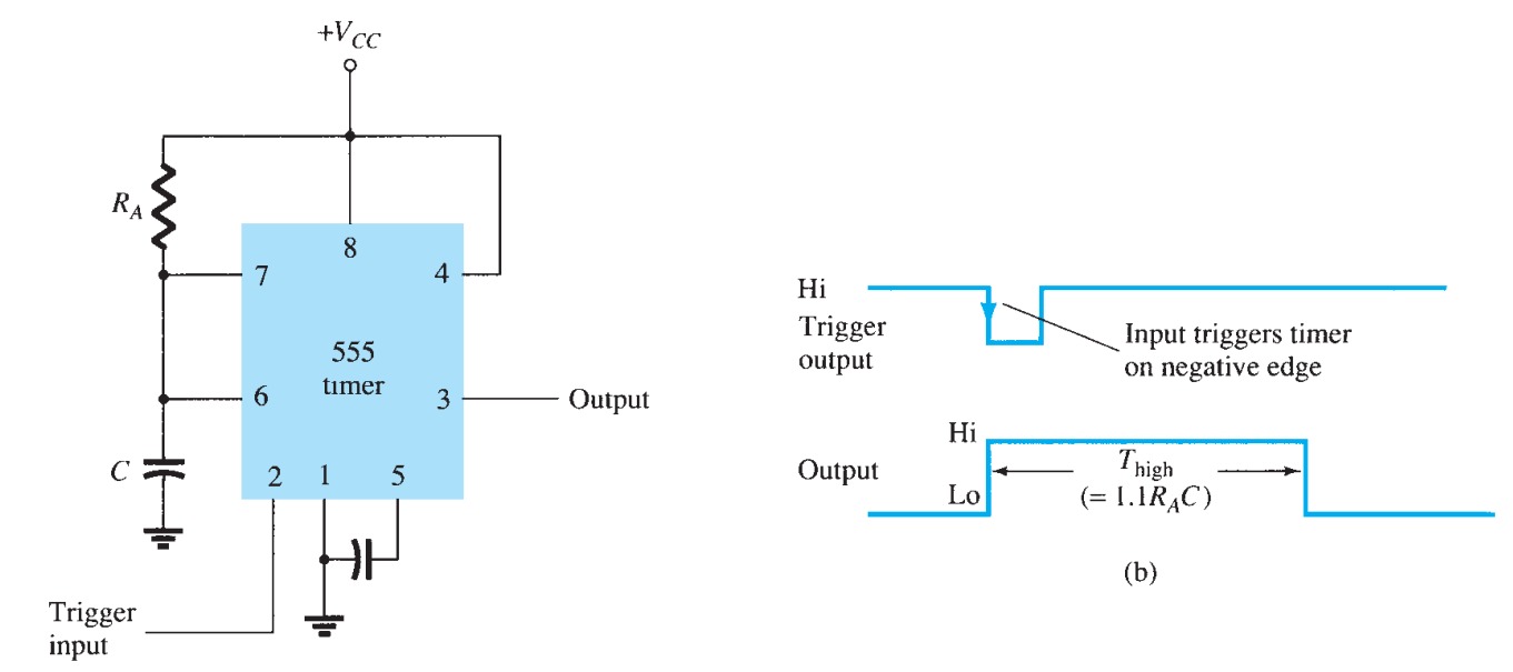
\[T_{\text{high}} = 1.1\, R_{A}C\]
Referring back to Fig. 13.16 , we see that the negative edge of the trigger input causes comparator 2 to trigger the flip-flop, with the output at pin 3 going high. Capacitor \(C\) charges toward \(V_{CC}\) through resistor \(R_A\) . During the charge interval, the output remains high. When the voltage across the capacitor reaches the threshold level of 2 \(V_{CC}\,\gt 3\), comparator 1 triggers the flip-flop, with output going low. The discharge transistor also goes low, causing the capacitor to remain at near 0 V until triggered again. Figure shows the input trigger signal and the resulting output waveform for the 555 timer operated as a one-shot. Time periods for this circuit can range from microseconds to many seconds, making this IC useful for a range of applications.
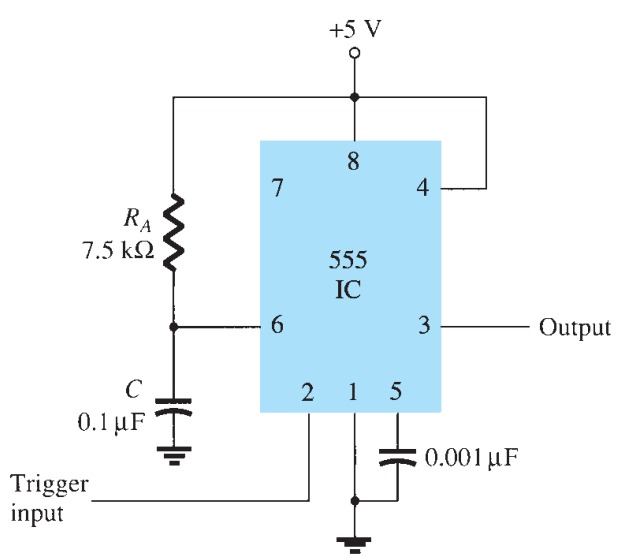
Example: Determine the period of the output waveform for the circuit of Fig. when triggered by a negative pulse.
Bistable Multivibrator
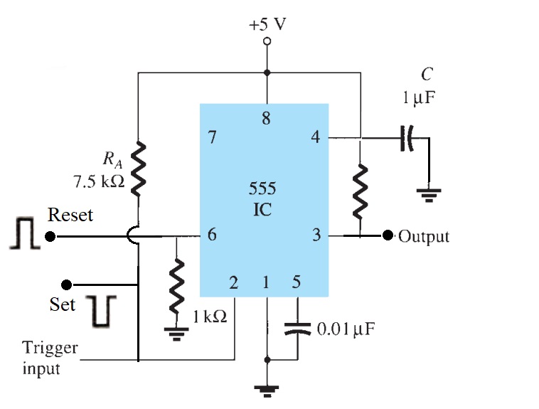
In these circuits, the output is stable in both the states. The states are switched using an external trigger but unlike the monostable multivibrator, it does not return back to its original state. Another trigger is needed for this to happen. This operation is similar to a flip-flop. There are no \(RC\) timing network and hence no design parameters. The following circuit can be used to design a bistable multivibrator. The trigger and reset inputs (pins 2 and 4 respectively on a 555) are held high via pull-up resistors while the threshold input (pin 6) is simply grounded. Thus configured, pulling the trigger momentarily to ground acts as a `set' and transitions the output pin (pin 3) to \(V_{CC}\) (high state). Pulling the threshold input to supply acts as a `reset' and transitions the output pin to ground (low state). No capacitors are required in a bistable configuration.