Teacher: Prof P. M. Sarun • NPHC206 • WINTER - 2025-2026 • Last updated:
Questions
A JFET has the following parameters: \(I_{\text{DSS}} = 32 \,\text{mA}\) ; \(V_{\text{P}} = – 8\,\text{V}\) ; \(V_{\text{GS}} = – 4.5 \,\text{V}\). Find the value of drain current.
A JFET has a drain current of \(5 \,\text{mA}\). If \(I_{\text{DSS}} = 10 \,\text{mA}\) and \(V_{\text{GS (off)}} = – 6 \,\text{V}\), find the value of (i) \(V_{\text{GS}}\) and (ii) \(V_{\text{P}}\).
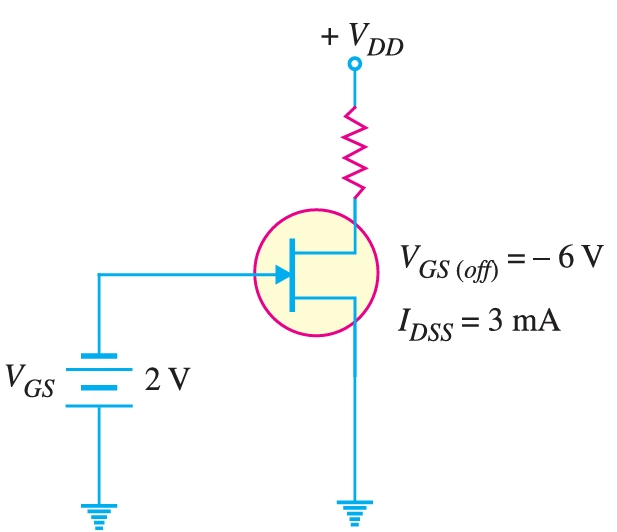
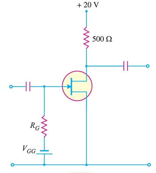
Determine the value of drain current for the circuit.
Figure 1.
What is the value of transconductance when \(V_{\text{GS}}\) of a JFET changes from \(–3.1 \,\text{V}\) to \(–3 \,\text{V}\), the drain current changes
from \(1 \,\text{mA}\) to \(1.3 \,\text{mA}\).
A JFET has a value of \(g_{\text{mo}} = 4000 \,\mu\text{S}\). Determine the value of \(g_{\text{m}}\) at \(V_{\text{GS}} = – 3\,\text{V}\). Given that \(V_{\text{GS (off)}} = – 8\,\text{V}\).
For a certain D-MOSFET, \(I_{\text{DSS}} = 10 \,\text{mA}\) and \(V_{\text{GS (off)}} = – 8\,\text{V}\). (i) Determine the channel of the device. (ii) Calculate \(I_{\text{D}}\) at \(V_{\text{GS}} = -3\,\text{V}\) and \(I_{\text{D}}\) at \(V_{\text{GS}} = +3\,\text{V}\).
The data sheet for an E-MOSFET gives \(I_{\text{D(on)}} = 500 \,\text{mA}\) at \(V_{\text{GS}} = 10\,\text{V}\) and \(V_{\text{GS (th)}} = 1\,\text{V}\). Determine the drain current for \(V_{\text{GS}} = 5\,\text{V}\).
Determine \(I_{\text{DSS}}\) in a D-MOSFET. Given \(I_{\text{D}} = 3 \,\text{mA}\), \(V_{\text{GS}} = – 2\,\text{V}\) and \(V_{\text{GS (off)}} = – 10\,\text{V}\).
How will you plot the transconductance curve for this E-MOSFET, when the The data sheet for an E-MOSFET gives \(I_{\text{D (on)}} = 3 \,\text{mA}\) at \(V_{\text{GS}} = 10\,\text{V}\) and \(V_{\text{GS (th)}} = 3\,\text{V}\).
Sketch the transfer curve for a p-channel JFET with \(I_{\text{DSS}} = 4 \,\text{mA}\) and \(V_{\text{P}} = 3 \,\text{V}\).
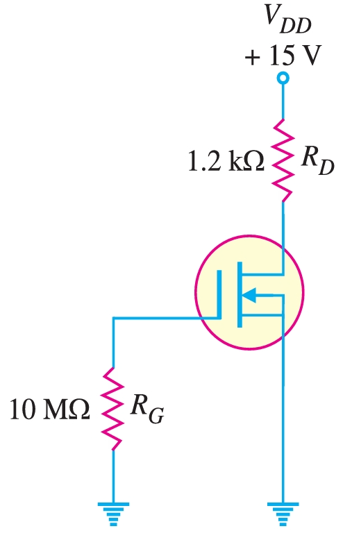
Determine \(V_{\text{DS}}\) for the circuit when \(I_{\text{DSS}} = 8 \,\text{mA}\).
Figure 2.
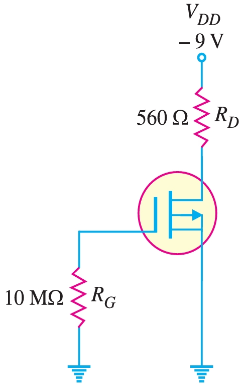
Determine \(V_{\text{DS}}\) for the circuit when \(I_{\text{DSS}} = 10 \,\text{mA}\)
Figure 3.
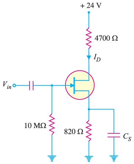
Find \(V_{\text{GS}}\) and \(V_{\text{DS}}\) in the JFET circuit shown in Fig. 4. Given, \(I_{\text{D}} = 1.9 \,\text{mA}\).
Figure 4.
Draw the d.c. load line for the JFET amplifier as shown in Fig 5.