Flip-Flops:
Flip-flops are fundamental building blocks in digital circuits, serving as memory elements that store binary information. These bistable devices have a wide range of applications, from basic memory storage to more complex sequential logic circuits. In this comprehensive exploration of flip-flops, we will delve into their types, operation, applications, and variations, shedding light on their significance in modern electronics.
Types of Flip-Flops
- SR Flip-Flop (Set-Reset Flip-Flop): The SR flip-flop has two inputs: Set (S) and Reset (R). It can store one bit of information, typically representing 0 or 1. Depending on the inputs, it can be in one of four states: Set, Reset, Hold, or Indeterminate. The latter occurs when both inputs are active simultaneously.
- JK Flip-Flop: The JK flip-flop is an evolution of the SR flip-flop, addressing the indeterminate state issue. It features J (Jump) and K (Kill) inputs, which allow for toggling and complementing the output respectively. It has four possible states: Set, Reset, Toggle, and Hold.
- D Flip-Flop (Data Flip-Flop): The D flip-flop has a single input, Data (D), which directly controls the output state. Its simplicity makes it useful in applications where synchronous memory elements are required.
- T Flip-Flop (Toggle Flip-Flop): The T flip-flop takes a Toggle (T) input. When the T input is high, the output toggles, making it useful for frequency division and generating square waves.
Operation Principles:
Flip-flops operate based on the principles of positive feedback and bistability. The key components in a flip-flop are logic gates (NAND, NOR, etc.) that control the state transitions. Each type of flip-flop has distinct input-output relationships and transition rules that determine how they store and manipulate information.
Applications of Flip-Flops"
- Memory Elements: Flip-flops serve as memory cells in registers and RAM. They retain data as long as power is supplied. The stability of their states makes them suitable for data storage and retrieval in digital systems.
- Sequential Logic Circuits: Sequential logic circuits rely on flip-flops to store and propagate information. Counters, shift registers, and finite state machines are examples of circuits that utilize flip-flops for sequential operation.
- Clock Synchronization: Flip-flops are often controlled by clock signals, ensuring synchronized operation within a digital system. This enables precise timing and coordination of various components.
- Frequency Division: T flip-flops are used to divide the frequency of an input signal by factors of 2. This property is valuable in clock generation and frequency synthesis.
S-R Flip-Flops:
Introduction to SR Flip-Flops:
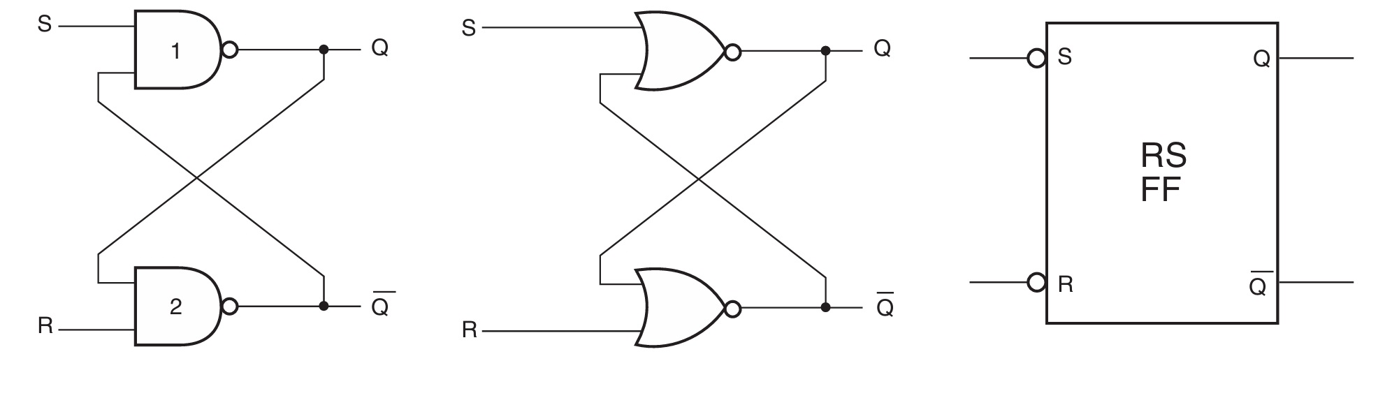
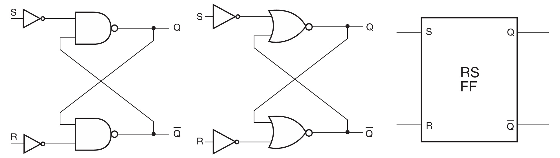
The S-R (Set-Reset) flip-flop is one of the simplest and most widely used. The S-R flip-flop consists of two inputs, the Set (S) and Reset (R) inputs, and two outputs, the Q and Q̅ outputs. The Q output represents the stored data bit, while Q̅ is its complement. The behavior of the S-R flip-flop is determined by its truth table, which outlines how it responds to various combinations of inputs.
Truth Table:
| S | R | Q(t) | Q̅(t) | Description |
|---|---|---|---|---|
| 0 | 0 | Q(t) | Q̅(t) | No change (hold state) |
| 0 | 1 | 0 | 1 | Reset |
| 1 | 0 | 1 | 0 | Set |
| 1 | 1 | ? | ? | Invalid state (ambiguous) |
In the truth table, \(Q(t)\) represents the current state of the \(Q\) output at time \(t\), and \(\overline{Q}(t)\) is its complement. The invalid state occurs when both S and R are set to 1 simultaneously, leading to unpredictable behavior.
Working Principles:
The S-R flip-flop operates based on the concept of cross-coupled NAND gates. When both S and R are 0, the flip-flop holds its state. When S is 1 and R is 0, the flip-flop is set (Q becomes 1, Q̅ becomes 0). Conversely, when S is 0 and R is 1, the flip-flop is reset (Q becomes 0, Q̅ becomes 1). When both S and R are 1, the flip-flop enters an ambiguous state, and this condition must be avoided.
Characteristics:
- Asynchronous Behavior: S-R flip-flops are asynchronous devices, meaning their outputs can change at any time in response to input changes, regardless of clock signals.
- Gated Operation: To control the timing of state changes, additional gating circuits are often added to S-R flip-flops. These gates ensure that the flip-flop responds only when certain conditions are met, enhancing stability.
- Race Conditions: Due to the asynchronous nature of S-R flip-flops, they are prone to race conditions. A race condition occurs when the outputs change unpredictably because different signals reach the flip-flop inputs at slightly different times.
- Feedback Loop: The cross-coupled NAND gates in an S-R flip-flop create a feedback loop. This loop maintains the state of the flip-flop until new input signals arrive.
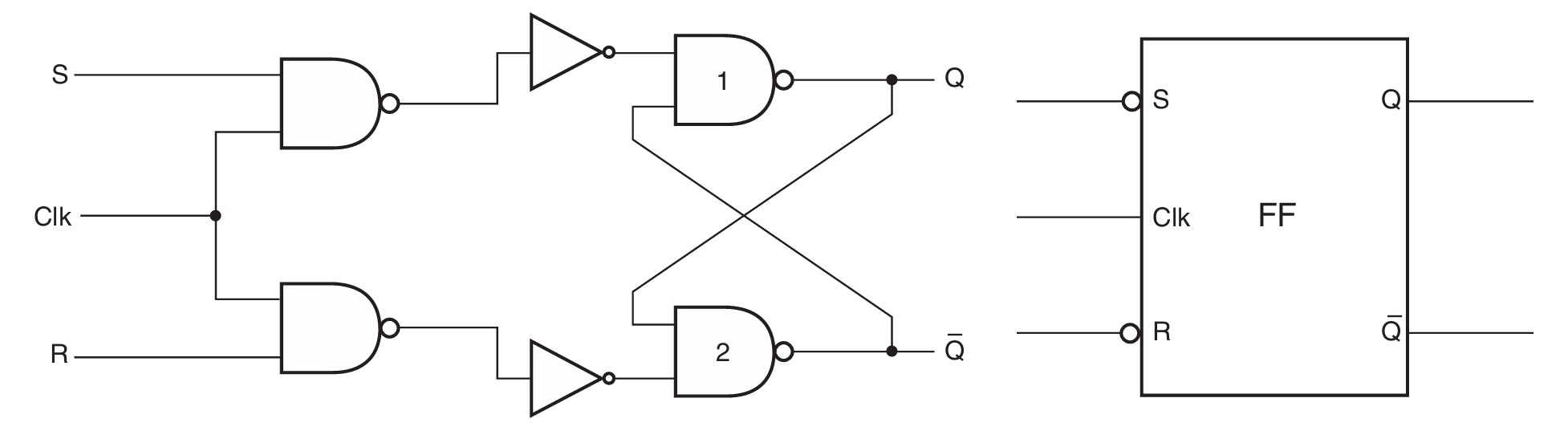
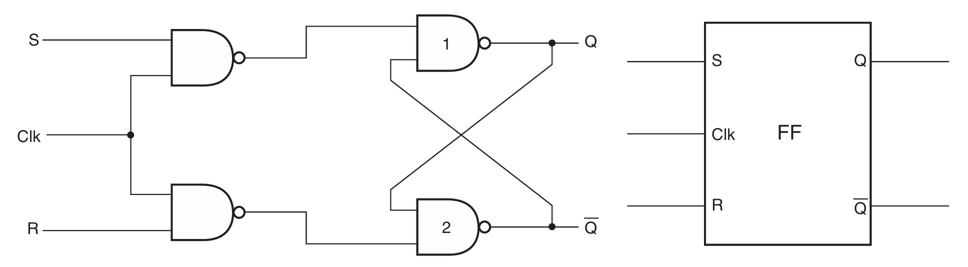
The behavior of an SR flip-flop can be summarized using its truth table:
| S | R | Q(t) | Q̅(t) | Description |
|---|---|---|---|---|
| 0 | 0 | Q(t) | Q̅(t) | No change |
| 0 | 1 | 0 | 1 | Reset |
| 1 | 0 | 1 | 0 | Set |
| 1 | 1 | 0 | 0 | Invalid (forbidden) |
Implementing SR Flip-Flops Using NAND Gates
NAND gates are versatile components in digital circuit design. They can be used to construct various logic gates and flip-flops. An SR flip-flop can be built using NAND gates, allowing for a deeper understanding of its internal workings.
1. SR Flip-Flop Construction
An SR flip-flop can be created using two NAND gates. The following is the implementation:
- Connect both S and R inputs to the respective inputs of the first NAND gate.
- Connect the output of the first NAND gate to both inputs of the second NAND gate.
- The output of the second NAND gate is Q̅, and its complement (Q) can be obtained by connecting Q̅ to an inverter.
2. Truth Table Validation
Let's validate the implementation using the truth table. Consider two NAND gates: NAND1 and NAND2. The inputs S and R are connected to the inputs of NAND1. The outputs of NAND1 and NAND2 are Q̅ and Q, respectively. The circuit's behavior aligns with the SR flip-flop truth table:
| S | R | NAND1 | NAND2 | Q(t+1) | Q̅(t+1) |
|---|---|---|---|---|---|
| 0 | 0 | 1 | 1 | Q(t) | Q̅(t) |
| 0 | 1 | 1 | 0 | 0 | 1 |
| 1 | 0 | 0 | 1 | 1 | 0 |
| 1 | 1 | 0 | 0 | 0 | 0 |
Limitation of SR Flip-Flop
SR flip-flops have some limitations. One of the main issues with the basic SR flip-flop is the possibility of entering the forbidden state (S=1, R=1). This state leads to unpredictable behavior and is usually avoided by introducing additional logic to ensure that the flip-flop transitions only occur as intended.
D Flip-Flops:
Introduction to Flip-Flops:
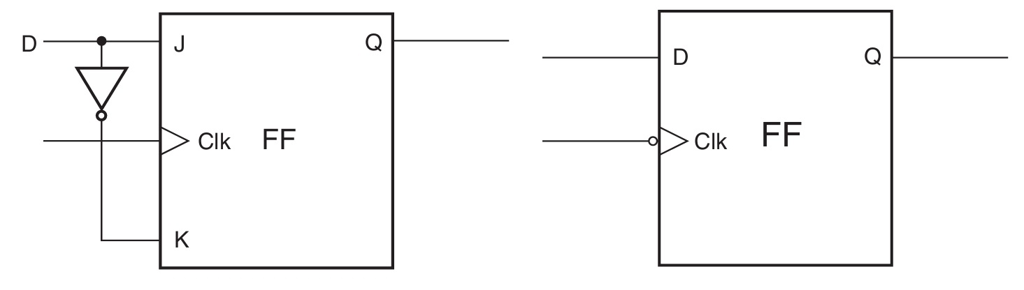
The D flip-flop, which is known for its simplicity and utility in various applications. The D flip-flop, also known as Data or Delay flip-flop, stores a single bit of data. It has two inputs: a D (data) input and a Clock (CLK) input. The output of the D flip-flop changes based on the value of the D input and the rising or falling edge of the clock signal.
A D flip-flop is a sequential circuit element that captures and stores a single binary bit of information. It has two stable states: SET and RESET. The main input to a D flip-flop is the "D" input, which represents the data to be stored. It also has a clock input (usually denoted as "CLK") that controls when the flip-flop reads and stores the data. When the clock signal transitions from low to high (rising edge), the D flip-flop samples the D input and updates its output accordingly.
D Flip-Flop Truth Table:
The truth table of a D flip-flop shows its behavior based on all possible input combinations. A D flip-flop truth table consists of four rows representing the possible combinations of D and CLK inputs and their corresponding Q (output) values. Here's the truth table for a D flip-flop:
| D | CLK | Q(t) | Q(t+1) |
|---|---|---|---|
| 0 | 0 | Q | Q |
| 0 | 1 | Q | 0 |
| 1 | 0 | Q | Q |
| 1 | 1 | Q | 1 |
Explanation of the Truth Table:
- When the D input is 0, the output Q remains unchanged regardless of the clock signal.
- When the D input is 1 and the CLK rises from 0 to 1 (rising edge), the output Q transitions from its current state to 1.
- When the D input is 1 and the CLK is 1, the output Q remains 1.
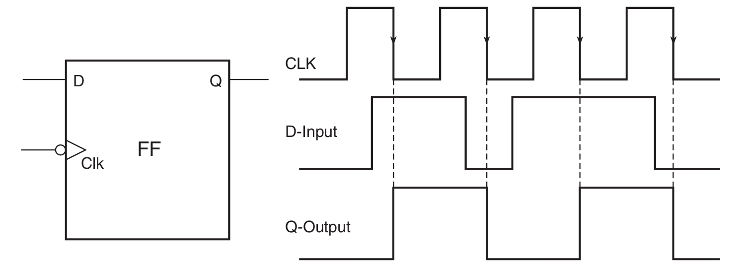
- When the D input is 1 and the CLK falls from 1 to 0 (falling edge), the output Q transitions from its current state to 0.
Characteristics of D Flip-Flops:
- Single Bit Storage: D flip-flops store a single bit of data, making them ideal for applications where only one bit needs to be stored or transferred.
- Edge-Triggered: D flip-flops are edge-triggered devices, meaning their output changes only on the rising or falling edge of the clock signal. This characteristic helps in synchronizing operations within digital circuits.
- Non-Volatile: D flip-flops are non-volatile, meaning they retain their state even after the power is turned off. This is crucial for maintaining data integrity in memory circuits.
- Synchronous Operation: The output of a D flip-flop changes synchronously with the clock signal, allowing for predictable and controlled timing behavior in sequential circuits.
Implementing D Flip-Flops using NAND Gates:
The D flip-flop can be constructed using NAND gates. Let's break down the implementation step by step:
- Flip Flop Structure: A simple way to implement a D flip-flop is by using a latch structure. A latch is an electronic circuit that can "latch" onto an input value and hold it until explicitly reset. Here, we'll use two NAND gates to create a latch-like behavior.
- Connect two NAND gates in a feedback loop (cross-coupled).
- Connect the output of one NAND gate to one input of the other NAND gate and vice versa.
- The "D" input is connected to one input of one of the NAND gates.
- The inverted output of the other NAND gate is the "Q" output of the flip-flop.
- Clock Input Integration: To create a D flip-flop that responds to the clock input, we'll need to add a clock control to the latch structure.
- Connect an additional NAND gate to one of the inputs of each of the NAND gates in the latch.
- Connect the clock input to one input of the newly added NAND gates.
- Connect the output of the existing NAND gate in the latch to the other input of the newly added NAND gates.
- Reset Functionality: To complete the D flip-flop implementation, we need to incorporate a reset mechanism.
- Add a NAND gate with one input connected to the "Q" output and the other input connected to the reset input.
- Connect the output of this NAND gate to the inputs of the existing NAND gates in the latch, ensuring that a reset signal propagates through the circuit when needed.
Behavior Analysis:
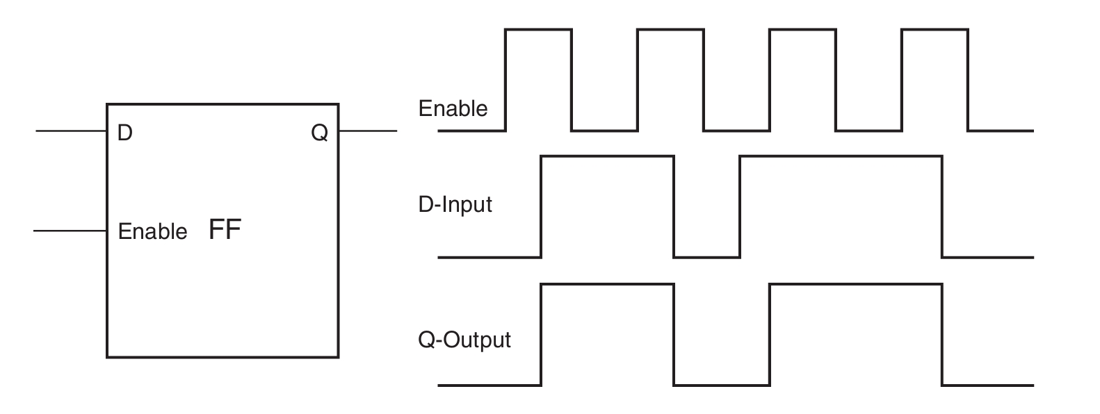
The truth table provided earlier summarizes the behavior of a D flip-flop. The flip-flop's output ("Q") follows the input data ("D") when the clock signal rises (CLK = 1). When the clock signal is low (CLK = 0), the flip-flop maintains its previous state.
When the clock transitions from low to high, the flip-flop captures the value of the D input and stores it. This behavior makes D flip-flops crucial components in sequential circuits like registers, counters, and memory cells.
Applications of D Flip-Flops:
D flip-flops find applications in various digital circuits, including but not limited to:
- Memory Elements: D flip-flops are used as memory elements in registers and memory units of processors and microcontrollers.
- State Machines: They are fundamental in designing finite state machines, which are essential components in control units and sequential logic circuits.
- Frequency Dividers: D flip-flops are employed in frequency divider circuits, where they divide the input clock frequency by a factor of 2.
- Shift Registers: In serial-to-parallel or parallel-to-serial data conversion, D flip-flops are used in shift registers to store and shift data.
- Data Synchronization: D flip-flops are used to synchronize data transfers between different clock domains in digital communication systems.