JK Flip-Flops:
Introduction
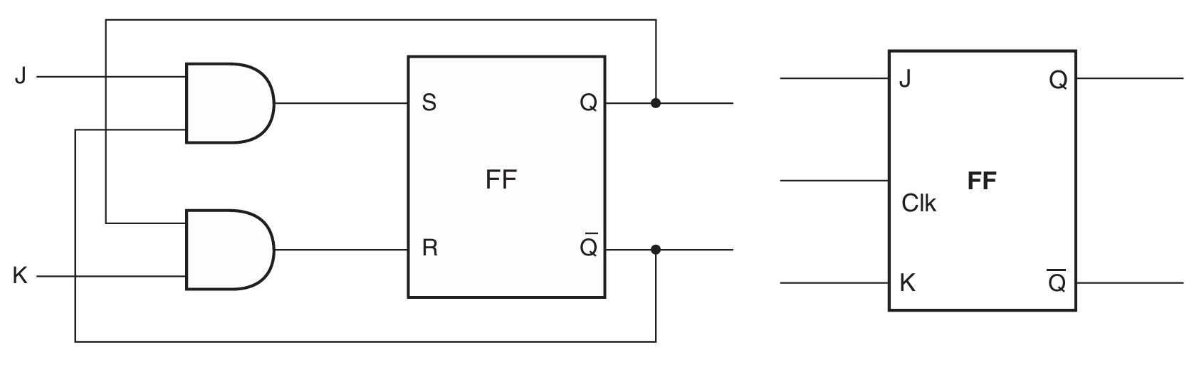
The JK flip-flop, with its versatile functionality and ability to toggle its output state, holds a prominent place in the realm of digital electronics. The JK flip-flop is named after its inventor, Jack Kilby. The JK flip-flop is an extension of the SR (Set-Reset) flip-flop. It overcomes the SR flip-flop's limitation of having an ambiguous state when both the Set and Reset inputs are active simultaneously. The JK flip-flop has two inputs: J (for "Jump") and K (for "Kill"). It has two outputs: Q (normal output) and Q' (complementary output). The primary feature that sets the JK flip-flop apart is its ability to toggle the output state, which makes it highly valuable in various applications.
Operation of JK Flip-Flop
The operation of a JK flip-flop can be understood through its characteristic truth table and state transition diagram.
Truth Table:
The JK flip-flop operates based on its inputs, clock signal, and current state. The truth table for a JK flip-flop outlines its behavior:
| J | K | C | Q(t) | Q(t+1) |
|---|---|---|---|---|
| 0 | 0 | X | Q | Q |
| 0 | 1 | ↑ | Q | 0 |
| 1 | 0 | ↑ | Q | 1 |
| 1 | 1 | ↑ | Q |
Here, 'X' denotes a don't-care condition, '↑' represents a rising edge of the clock signal, 'Q(t)' is the current state, and 'Q(t+1)' is the next state.
State Transition Diagram:
Explanation of Truth Table Entries:
- When both J and K are 0, the flip-flop retains its current state (no change).
- When J is 0 and K is 1, the flip-flop is forced to reset (Q becomes 0).
- When J is 1 and K is 0, the flip-flop is forced to set (Q becomes 1).
- When both J and K are 1, the flip-flop toggles its state.
Analysis of the Truth Table
The provided truth table illustrates the behavior of a JK flip-flop under different input conditions. Let's delve deeper into the table:
- J = 0, K = 0: The flip-flop remains in its current state, as there are no inputs to alter it. This property is essential for memory retention.
- J = 0, K = 1: The flip-flop is forced to reset, setting Q to 0. This can be useful for controlled data clearing or initialization.
- J = 1, K = 0: The flip-flop is forced to set, changing Q to 1. This is useful for initializing the flip-flop with specific data.
- J = 1, K = 1: This configuration causes the flip-flop to toggle its state. It alternates between 1 and 0 on successive clock pulses, effectively creating a frequency divider.
J-K Flip-Flop with PRESET and CLEAR Inputs
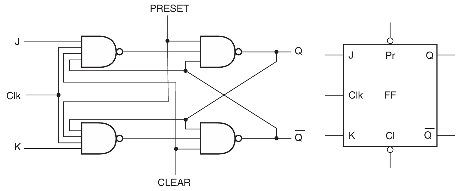
In many sequential logic applications, it becomes essential to forcibly set a J-K flip-flop to a known starting state, either by clearing it to a logic 0 or presetting it to a logic 1, independent of the normal clocked operation. This is achieved through two additional asynchronous inputs-CLEAR and PRESET-which, in this particular implementation, are both active when they are at a low logic level. When the CLEAR input is held at logic 0 while the PRESET remains at logic 1, the output Qn is immediately forced to 0, regardless of the clock signal or the current values on the J and K inputs. Conversely, applying a logic 0 to the PRESET input while keeping CLEAR at logic 1 instantly sets the output to 1, again overriding any clock-dependent behavior. In both cases, the action takes effect as soon as the active low level is applied, without waiting for a clock edge, because these inputs have the highest priority in the circuit.
During normal clocked operation, both PRESET and CLEAR must be held at logic 1 (their inactive state), allowing the flip-flop to respond solely to the J, K, and clock inputs according to the standard function table. A critical design rule to remember is that the two active-low inputs should never be activated simultaneously-that is, PRESET and CLEAR must not both be logic 0 at the same time-because this creates a conflicting internal condition where the circuit attempts to drive the output to both 1 and 0 concurrently, leading to an unpredictable or undefined output state. Therefore, proper initialization requires applying either the preset or clear condition briefly, then releasing both to their inactive high state before proceeding with clocked operations.
Master–Slave J-K Flip-Flops
A common reliability issue in flip-flop operation arises when the clock pulse width exceeds the propagation delay of the device. Under such conditions, the output state change becomes unpredictable, as the circuit cannot settle properly within the clock interval. In edge-triggered flip-flops, the relevant timing parameter is actually the narrow trigger pulse generated internally by the edge-detection circuitry, rather than the overall width of the external clock signal. This undesirable behavior is widely known as the race problem, and because propagation delays in modern digital circuits are typically extremely small, the chance of encountering such a race condition is actually quite high, making it a practical concern in many designs.
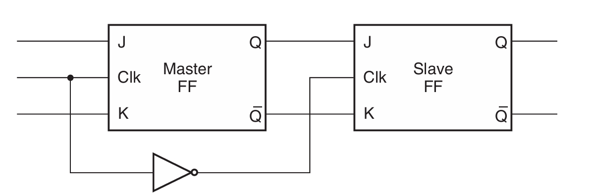
To overcome this limitation, engineers developed the master–slave configuration, which effectively decouples the input sensing from the output updating. This structure consists of two cascaded J-K flip-flops: the first, called the master, receives the external inputs, while the second, called the slave, produces the final output. The crucial feature is that the clock signal fed to the slave is the logical complement of the clock applied to the master. As a result, when the clock is high, the master is enabled and can change its state according to the J and K inputs, but the slave remains disabled and holds its previous output. Conversely, when the clock goes low, the master becomes disabled and stops responding to the inputs, while the slave is now enabled and updates its output to match the state that was captured in the master. In this way, the contents of the master are transferred to the slave only during the low portion of the clock cycle, ensuring that any new input changes occurring after the master is disabled do not affect the output until the next full clock period.
From this description, it becomes evident that a master–slave flip-flop is fundamentally a pulse-triggered device rather than an edge-triggered one, since its state transition takes place over the entire duration of the clock pulse rather than on a single rising or falling edge. A typical function table for such a flipflop includes active-low PRESET and CLEAR inputs for asynchronous initialization, alongside active-high J and K inputs for normal operation. Despite its historical significance and its effectiveness in solving the race problem, the master–slave configuration has largely fallen out of use in contemporary digital design, having been superseded by more robust edge-triggered designs that offer better speed, simpler timing constraints, and greater immunity to glitches.
T Flip-Flops:
Introduction
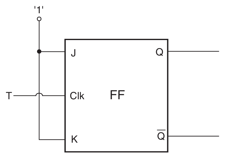
The T flip-flop, also known as the Toggle flip-flop. The T flip-flop is a modification of the JK flip-flop, designed to simplify certain operations. The T flip-flop has a single input known as the "Toggle" input (T). When the Toggle input is asserted, the flip-flop switches its state (from 0 to 1 or vice versa), hence the name "Toggle" flip-flop. The T flip-flop can be implemented using both digital logic gates and integrated circuits. Its ability to toggle its output state based on the input signal has led to a wide range of applications in frequency division, toggling logic, state machines, frequency synthesis, and pulse generation.
T Flip-Flop: Truth Table
The truth table of a \(T\) flip-flop illustrates its behavior based on the input \(T\) and the current state \(Q\). The \(Q\) represents the output state of the flip-flop. The \(T\) flip-flop truth table is as follows:
| T | Q(t) | Q(t+1) |
|---|---|---|
| 0 | 0 | 0 |
| 0 | 1 | 1 |
| 1 | 0 | 1 |
| 1 | 1 | 0 |
In this truth table, \(Q(t)\) represents the current state of the flip-flop, while \(Q(t+1)\) represents the next state after the clock cycle. The \(T\) input determines whether the state toggles or remains the same.
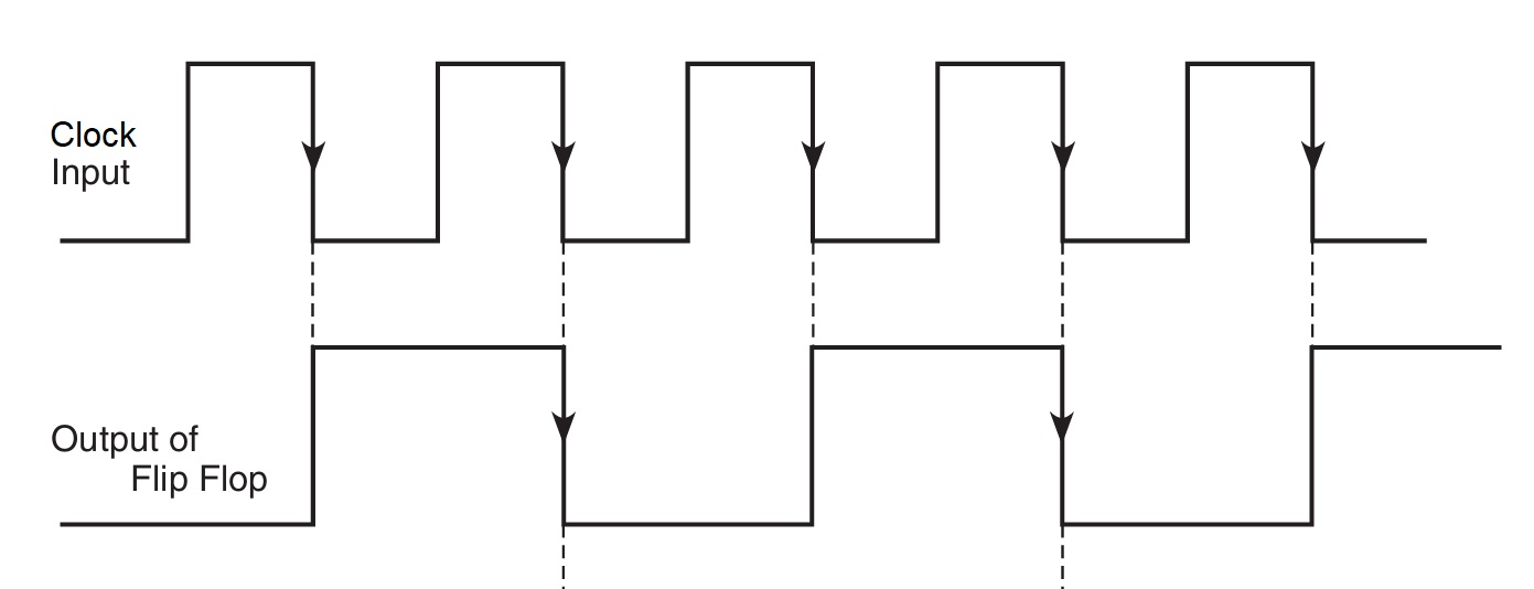
T Flip-Flop: Timing Diagram
A timing diagram visually represents the behavior of a \(T\) flip-flop over multiple clock cycles. It illustrates the changes in input, output, and clock signals, allowing designers to analyze the flip-flop's operation and stability.
T Flip-Flop: Applications
- Frequency Division: \(T\) flip-flops are commonly used in frequency dividers. By connecting multiple \(T\) flip-flops in a cascade, a counter can be created that divides the input frequency by \(2^n\), where \(n\) is the number of flip-flops.
- Toggling Logic: The inherent toggling behavior of the \(T\) flip-flop is useful in creating toggling circuits. These circuits can generate square wave outputs, which are commonly employed in clock generation and signal processing.
- State Machines: \(T\) flip-flops play a pivotal role in designing state machines, which are used to control sequential logic circuits. State machines find applications in various fields, including digital control systems and communication protocols.
- Frequency Synthesis: \(T\) flip-flops are used in frequency synthesis circuits to generate a frequency that is a multiple of a reference frequency. This technique is crucial in generating stable and accurate clock signals for microprocessors and communication systems.
- Pulse Generators: \(T\) flip-flops can be used to generate precise width pulses. By appropriately setting the \(T\) input and clock frequency, one can create pulses with specific durations for various applications like triggering events and synchronization.