Semiconductors
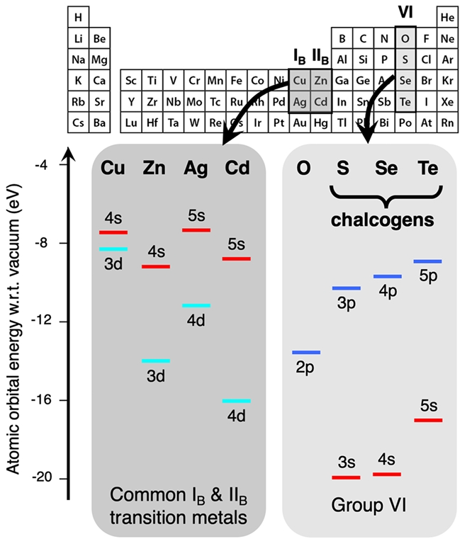
Semiconductors are the materials at the heart of many electronic devices. The elemental semiconductors are few, the only ones of any practical use being germanium (\(Ge\)) and silicon (\(Si\)) and only silicon is widely used nowadays. However, there are some compound semiconductors which find applications in light-emitting diodes, semiconductor lasers, microwave devices and other specialised areas. Most of these are based on elements from groups \(III\) and \(V\) of the periodic table and occasionally from groups \(II\) and \(VI\). These are known respectively as \(III-Y\) and \(II-VI\) compounds, examples being gallium arsenide (\(GaAs\)), gallium phosphide (\(GaP\)) and cadmium sulphide (\(CdS\)). The Semincondcting elements available in the Periodic Table are \(B\), \(C\), \(Si\), \(Ge\), \(As\), \(Se\), and \(Te\).
Electrons and holes
Semiconductors are only different from insulators because of conduction brought about by thermally generated charge carriers (intrinsic conduction) or by the addition of controlled amounts of impurities (extrinsic conduction), called dopants. In semiconductor devices only extrinsic conduction is desirable. The charge carriers are electrons and holes, which act just like positively-charged electrons. By adding the right kind of dopants it is possible to make semiconductor material which conducts either with electrons alone (\(n\)-type material) or with holes alone (\(p\)-type material). But first we must consider the ordinary processes of electrical conduction.
Electrical conductivity
The resistance, \(R\), of a bar of material of length, \(l\), and uniform cross-sectional area, \(A\), is
\[R = l/\sigma A\]
where \(\sigma\) is the electrical conductivity of the material. If \(l\) is in \(m\), \(A\) in \(m^{2}\) and \(R\) in \(\Omega\), then \(\sigma\) is in \(S/m\). The reciprocal of the conductivity is the resistivity, \(\rho\), which has units of \(\Omega m\).
The electrical conductivity of materials is found to vary over a very wide range - wider than any other material property. Materials came to be classified according to the behaviour and magnitude of their conductivities. Some, mainly metals and alloys, were found to be good conductors at room temperature (\(\rho\) ranging from about \(10^{-8}\) for silver to \(10^{-6}\) \(\Omega m\) for nichrome resistance wire), with a conductivity which decreased with increasing temperature and did not change much when the metal was impure. Other materials, mainly non-metals such as sulphur, polystyrene and silica, were found to have a very low conductivity at room temperature (\(\rho = 10^{10}\) to \(10^{16}\) \(\Omega m\)) which increased rather rapidly with temperature.
Again it was found that the purity of the material had relatively little effect on the conductivity or its temperature coefficient. Then there was another class of materials, such as germanium, silicon and silicon carbide, which had very variable conductivities (\(\rho = 10^{-6}\) to \(10^{2}\) \(\Omega m\)) and temperature coefficients that could be positive or negative and depended, it was eventually discovered, on the kind of impurities present, sometimes only in tiny amounts. Though these materials came to be called semiconductors, there is no fundamental difference between insulators and semiconductors: diamond is widely considered to be an insulator, and mostly it is, but semiconducting diamonds are known. Finally a fourth type of material was discovered (by Kammerlingh Onnes in 1911) that had no resistance at all below a critical temperature: it was a superconductor.
Intrinsic semiconductor
Generally speaking the conductivity of metals is due to free electrons in them and these are largely absent from semiconductors. There does, however, appear to be a characteristic energy associated with the conduction process. If sufficiently energetic photons (quanta of e.m. radiation) are incident on a semiconductor its conductivity rises enormously. The photon's energy can be equated with the energy needed to transfer an electron from a bound state (the electron is said to be in the valence band) to a free or conducting state (then it is said to be in the conduction band). This characteristic energy is known as the band-gap energy or just the band gap.
Measurements in magnetic fields (Hall-effect measurements) show that there are two types of charge carrier: a negatively charged one identified with the electron and a positively charged one called a hole. When a photon causes an electron to transfer from valence band to conduction band it leaves behind a hole in the valence band. This hole can move under the influence of an electric field, that is it is a charge carrier that acts like a positively charged electron.
Silicon has a band gap of about \(1.1 ~eV\) (electron volts, \(1 ~eV = 1.6 \times 10^{-19} J\)), meaning that an electron (charge, \(-q = -1.6 \times 10^{-19} C\)) changes its potential by \(1.1 V\) on crossing the band gap. Germanium has a band gap of \(0.7 ~eV\) and diamond has one of \(5.4 ~eV\). Thermal energy can also cause the creation of electron-hole pairs that causes conduction. In a pure semiconductor kept in the dark, thermally generated charge carriers are the sole means of conduction. The numbers of them per unit volume (the intrinsic carrier concentration, \(n_{i}\) are given by
\[n_i = N~exp\left(\frac{-E_g}{2k_BT}\right)~~~~~~~~~~~~~~~~~~~~~~~~(1)\]
where \(N\) is a constant for a given semiconductor, \(E_{g}\) is the band gap energy in Joules, \(k_{B}\) is Boltzmann's constant (\(1.38 \times 10^{-23}~J/K\)) and \(T\) is the temperature in \(K\). The factor of \(2\) in the denominator of the exponent means that in classical terms, the electron starts off in the middle of the band gap. This is because electrons are not classical particles. Be that as it may, no matter how carefully prepared the material is, there will always be thermal carrier generation and associated conductivity.
The conductivity in any material is given by \(\sigma = nq \mu\), where \(\mu\) is the mobility of the charge carrier. The mobility is the speed (\(v\)) that a charge carrier acquires per unit electric field (\(E\)), that is \(\mu = v/E\). \(q\) is the magnitude of the electronic charge and n the number of charge carriers per unit volume. For an intrinsic semiconductor
\[\sigma =nq(\mu_{e} +\mu_{h})~~~~~~~~~~~~~~~~~~~~~~~~(2)\]
where \(n\) is the number of electron-hole pairs and \(\mu_{e}\) and \(\mu_{h}\) are the respective electron and hole mobilities. It is worthwhile putting some numbers into equations 1 and 2. The material constants for silicon are \(N = 3 \times 10^{25}/m^{3}\), \(E_{g} = 1.1~~eV\) = \(1.76 \times 10^{-19}~J\), \(\mu_{e} = 0.14 m^{2}V^{-1}~s^{-1}\) and \(\mu_{h} = 0.05~m^{2}V^{-1}s^{-1}\), so at \(300~K\), equation \(2\) yields \(n_i= 2 \times 10^{16}~m^{-3}\) and equation \(3\) gives \(\sigma= 6 \times 10^{-4}~S/m\) or \(p = 1/\sigma = 1650~\Omega m\). A bar of intrinsic silicon \(100~mm\) long and of square cross-section, \(10\) mm by \(10\) mm, would then have, by equation 1, a resistance of \(1.7 M\Omega\). Compare this with a copper bar of the same size, which would have a resistance of \(17 \mu\Omega\). Equation 2 also shows that the carrier density and hence a will rapidly increase with temperature (by \(7 \%/K\)).
Extrinsic semiconductor
At 300 K the intrinsic carrier concentration is not very high in silicon and the numbers of electrons and holes are equal. Silicon is a covalently-bonded element with the same structure as diamond and germanium. Each silicon atom has four outer, bonding electrons and with them it forms four covalent bonds by which it is joined to four other silicon atoms arranged at the comers of a regular tetrahedron as in figure.
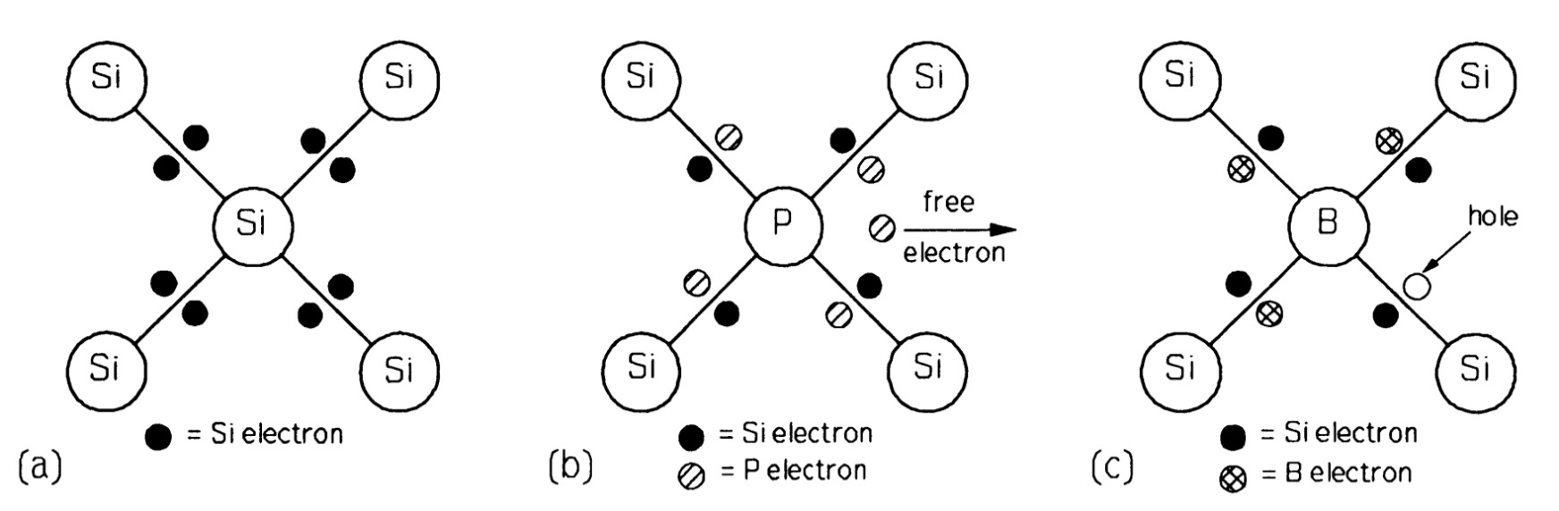
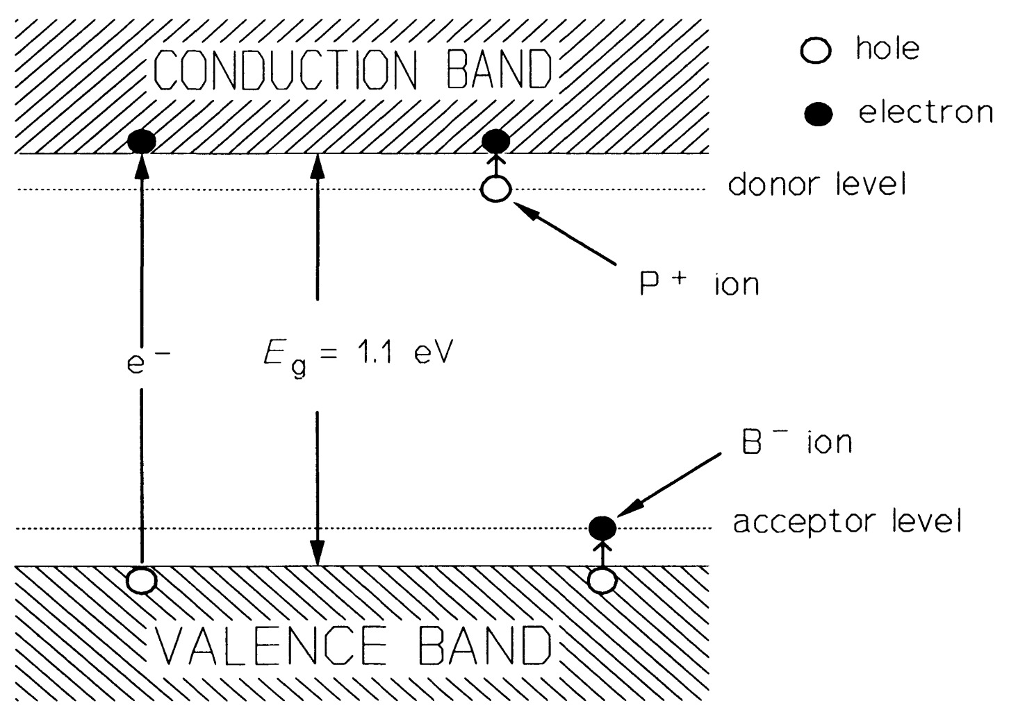
If an atom of silicon is replaced by one of phosphorus, which has five electrons available for bonding, then it can form four bonds with neighbouring silicon atoms, using up four electrons and having one left over. This spare electron is readily detached from its parent atom (the ionisation energy is of the order of \(10 m~eV\)) to move into the nearby conduction band; at \(300 K\) practically all the phosphorus atoms are ionised. The concentration of phosphorus atoms, \(N_{D}= n\), the conduction-electron concentration. Phosphorus is known as a donor atom because it donates electrons to the conduction band. Arsenic and antimony behave as donors in silicon too.
When an atom of boron is substituted for one of silicon the position is different, as boron has only three electrons available for bonding, as a result, when it forms four bonds with a neighbouring silicon atom as in figure, there is a deficiency of an electron -a hole - in one of the bonds. This hole can also move about freely in the valence band and acts as a mobile positive charge carrier, though really the electrons move the other way. The boron atoms are also effectively \(100 \%\) ionised in silicon (though negatively, not positively like phosphorus), so the concentration of boron atoms, \(N_{A}= p\), the hole concentration. Boron is termed an acceptor because it accepts an electron from a silicon atom. In semiconductor devices, the dopant atom concentration far exceeds the intrinsic carrier density; conduction is thus said to be extrinsic. Figure shows the energy levels in extrinsic silicon. The higher up an electron is in figure , the higher is its energy. However, for holes, the lower it is, the higher is its energy.
The law of mass action applies to the charge carrier concentration in a semiconductor, that is the product of electron and hole concentration, \(p-n\), is constant at constant temperature. If electrons predominate, the material is said to be \(n\)-type and the electrons are the majority carriers, holes the minority carriers. If holes predominate, the material is \(p\)-type, holes are the majority and electrons the minority carriers.
Effect of Temperature
The electrical conductivity of a semiconductor changes appreciably with temperature variations.
At absolute zero.
At absolute zero temperature, all the electrons are tightly held by the semiconductor atoms. The inner orbit electrons are bound, whereas the valence electrons are engaged in covalent bonding. At this temperature, the covalent bonds are very strong, and there are no free electrons. Therefore, the semiconductor crystal behaves as a perfect insulator.
In terms of energy band description, the valence band is filled, and a large energy gap exists between the valence band and the conduction band. Therefore, no valence electron can reach the conduction band to become a free electron. It is due to the non-availability of free electrons that a semiconductor behaves as an insulator.
Above absolute zero.
When the temperature is raised, some of the covalent bonds in the semiconductor break due to the thermal energy supplied. The breaking of bonds sets those electrons free that are engaged in the formation of these bonds. The result is that a few free electrons exist in the semiconductor. These free electrons can constitute a tiny electric current if a potential difference is applied across the semiconductor crystal. This indicates that the resistance of a semiconductor decreases with an increase in temperature, i.e., it has a negative temperature coefficient of resistance. It may be added that at room temperature, current through a semiconductor is too small to be of any practical value.
As the temperature is raised, some of the valence electrons acquire sufficient energy to enter the conduction band and thus become free electrons. Under the influence of an electric field, these free electrons will constitute an electric current. It may be noted that each time a valence electron enters the conduction band, a hole is created in the valence band. The holes also contribute to the current.
At room temperature, some of the covalent bonds in pure semiconductor break, setting up free electrons. Under the influence of an electric field, these free electrons constitute an electric current. At the same time, another current – the hole current – also flows in the semiconductor. When a covalent bond is broken due to thermal energy, the removal of one electron leaves a vacancy, i.e., a missing electron in the covalent bond. This missing electron is called a hole, which acts as a positive charge. Hole acts as a virtual charge, although there is no physical charge on it.
For one electron set free, one hole is created. Therefore, thermal energy creates hole-electron pairs; there are as many holes as the free electrons. The current conduction by holes can be explained as follows :
When the valence electron becomes a free electron due to thermal energy, it creates a hole in the covalent bond of the atom. The hole is a strong centre of attraction for the electron. A valence electron from a nearby covalent bond comes to fill in the hole. This results in the creation of a hole at the neighbouring location from where the electron came. Another valence electron, in turn, may leave its bond to fill the previous hole, thus creating a new hole. Thus, the hole with a positive charge has moved from one location in the solid to another, i.e., towards the negative terminal of the supply. This constitutes the Hole current. Hole current is due to the movement of valence electrons from one covalent bond to another bond.
The temperature dependence of the resistivity of semiconductors and insulators is given by the following formula :-
\[\rho(T) = \rho_0~e^{-\frac{E_g}{k_B T}}\]
where, \(E_g\) is the energy gap between conduction band and valance band, \(k_B\) is the Boltzmann's constant, \(T\) is the temperature and \(\rho(T)\) and \(\rho_0\) is the resistivity of the material as temperature T (in Kelvin) and at zero Kelvin, respectively.
Majority and Minority Carriers
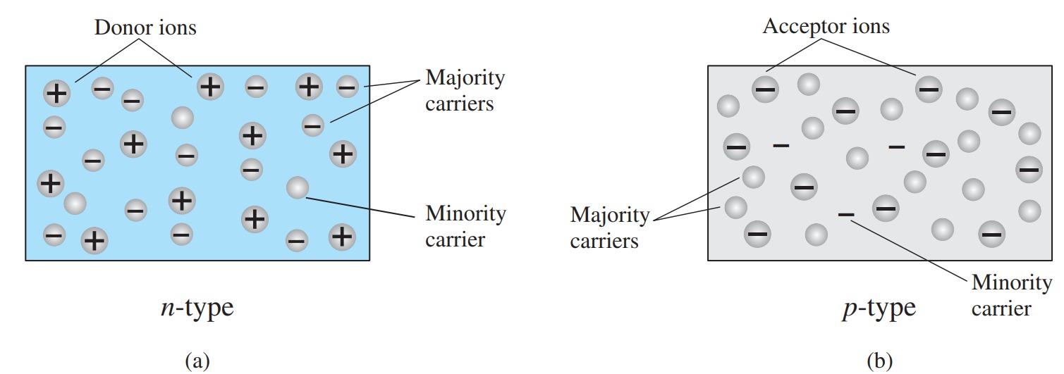
In the intrinsic state, the number of free electrons in Ge or Si is due only to those few electrons in the valence band that have acquired sufficient energy from thermal or light sources to break the covalent bond or to the few impurities that could not be removed. The vacancies left behind in the covalent bonding structure represent our very limited supply of holes. In an n-type material, the number of holes has not changed significantly from this intrinsic level. The net result, therefore, is that the number of electrons far outweighs the number of holes. For the p-type material, the number of holes far outweighs the number of electrons. For this reason:
In an n-type material, the electron is called the majority carrier and the hole the minority carrier.
In a p-type material, the hole is the majority carrier, and the electron is the minority carrier
When the fifth electron of a donor atom leaves the parent atom, the atom remaining acquires a net positive charge, hence the plus sign in the donor-ion representation. For similar reasons, the minus sign appears in the acceptor ion. The n - and p-type materials represent the basic building blocks of semiconductor devices.
The p-n junction
Whether a particular piece of semiconductor is \(p\)-type, \(n\)-type or intrinsic makes no difference to the direction of (conventional) current flow when a voltage is applied to its ends, though the current's magnitude will depend on the doping level. But when \(p\)- and \(n\)-type materials are joined, or a \(p-n\) junction is formed, matters undergo a great transform-ation: current is now found to flow much more easily in one direction than in the other. The junction is a rectifier, or diode. \(p-n\) junctions, singly or in combinations of two or more, are essential for the operation of many semiconductor devices.
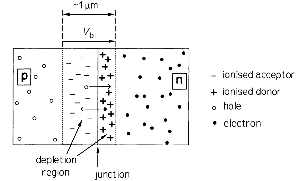
Figure 1 shows a cross-section of a \(p-n\) junction, with no externally applied potential.
Before the junction is formed the \(n\)-type material consists of fixed, positively-charged donor ions and an equal number of conduction electrons, while the \(p\)-type material consists of fixed, negatively-charged acceptor ions and an equal number of holes. When the junction is formed, electrons from the \(n\)-type region diffuse into the \(p\)-type region (leaving a fixed positive charge behind) and combine with holes. Simultaneously, holes from the \(p\)-type region diffuse into the \(n\)-type region (leaving a fixed negative charge behind) and combine with free electrons, thus causing an absence of mobile charge carriers in the junction region. In the depletion region (or zone) in the vicinity of the junction a voltage called the built-in potential, \(V_{bi}\) is thus set up which opposes the diffusion of charge carriers across the junction. \(V_{bi}\) is about \(0.6~V\) in silicon, about \(1.2 ~V\) in \(GaAs\) and about \(0.3 ~V\) in germanium. Thus with no bias applied, the diffusion current for the electrons (from then-region), \(I_{er}\) is exactly equal to the current (due to thermally generated electrons in the \(p\)-region), \(I_{eg}\) produced by \(V_{bi}\)· The same is true for the hole currents, \(I_{hg}\) and \(I_{hr}\). The holes and electrons move in opposite directions, though the conventional currents are in the same direction because of the negative electronic charge:
Thus
\[I_{ g} = I_{eg} + I_{hg}\].
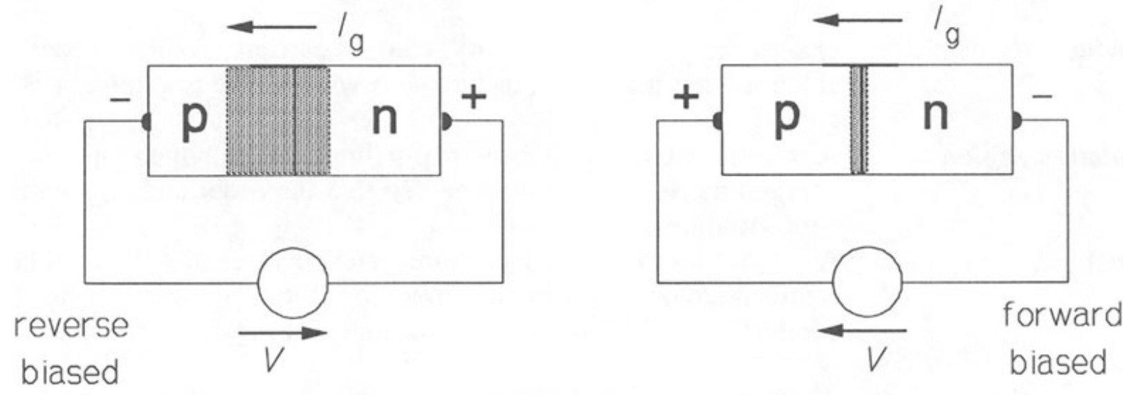
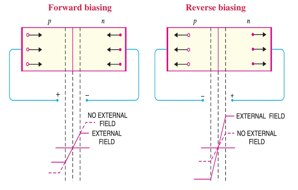
When reverse bias is applied to the junction, that is the \(p\)-type side is made more negative than the \(n\)-type, the depletion region becomes larger as the bias voltage adds to \(V_{bi}\). The diffusion current, \(I_{r}\) that flows across the junction is very small, since only carriers with enough energy can surmount the potential barrier. But the current, \(I_{g}\), due to thermally generated minority carriers, remains unaffected by the bias field, resulting in a net reverse current, \(I_{g} - I_{r}\). When the junction is fotward biased (\(p\)-type side positive with respect to the \(n\)-type) the depletion zone is narrower than under zero bias and \(I_{r}\) is now very much greater than \(I_{g}\). Figure shows the effect of bias polarity on the depletion zone widths and the forward current.
Reverse current is often called leakage current and its magnitude depends on the material and the size of the diode. Germanium diodes have high leakage currents - about \(1,000\) times that of silicon diodes (a silicon signal diode at room temperature typically has a leakage of around \(1 nA\)). Light causes the generation of additional electron-hole pairs in semiconductors thereby increasing the leakage current. The so-called dark current is the leakage current when no light falls on the semiconductor material.
A glossary of terms
| Terms | Details |
|---|---|
| Acceptor | A dopant atom that has fewer valence electrons than the host semiconductor material, so that it can accept one or more electrons from the valence band of the host and gives rise to a corresponding number of holes in the valence band. Boron is an acceptor atom in silicon |
| Band gap | The energy difference, \(E_{g}\), between the top of the valence band and the bottom of the conduction band, usually given in electron volts (\(~eV\)), where \(1 ~eV = 1.6 \times 10^{-19} J\). In silicon the band gap is about \(1.1 ~eV\). |
| Bias | The potential applied to a \(p-n\) junction. Positive bias means that the \(p\)-type side of the junction is at a higher potential than the \(n\)-type side, negative bias means vice versa |
| Charge carrier compensation | Either a negatively-charged electron or a positively charged hole The reduction in charge-carrier concentration in a semiconductor that is brought about by incorporating both donors and acceptors into the semiconductor material. Hence reduced conductivity |
| Conduction band | A region of energy states lying above the valence band and separated from it by an energy gap in which electrons are not bound to their parent atoms and can move under the influence of applied fields |
| Conductivity | Defined by \(\sigma= nq\mu\), where \(n\) = charge carriers/\(m^{3}\), \(q\), the electronic charge = \(1.6 \times 10^{-19} C\), \(\mu\) = mobility (\(q.v.\)) in \(m^{2}/V/s\). The reciprocal of the resistivity (\(q.v.\)) |
| Conductivity type | Determined by the majority charge carriers. When these are electrons the material is \(n\)-type and when these are holes it is \(p\)-type |
| Depletion region | A volume of material near a \(p-n\) junction in which oppositely charged carriers have combined so that the mobile charge carrier concentration is very small |
| Donor | A dopant atom which has more valence electrons than its host semiconductor, so that it tends to give up electrons to the conduction band, so making the material \(n\)-type. Examples are phosphorus and arsenic in silicon |
| Dopant | An element which is incorporated in controlled amounts into a semiconductor during crystal growth. At working temperatures the dopant is ionised and supplies electrons or holes to the host to produce a vast excess of one or the other, so making the material \(p\)-type or \(n\)-type |
| Extrinsic conduction | Conduction brought about by charge carriers from ionised dopants |
| Hole | The absence of an electron in the valence band, which acts like a positively charged electron |
| Intrinsic conduction | Conduction by hole-electron pairs produced by ionisation of the semiconductor material. Ionisation means that electrons in the valence band must cross the band gap to reach the conduction band. At normal temperatures there are few carriers produced like this and conductivity is low |
| Majority carrier | The more-numerous charge-carrier. Electrons in \(n\)-type material, holes in \(p\)-type |
| Minority carrier | The less-numerous charge-carrier. Holes in \(n\)-type material, electrons in \(p\)-type |
| Mobility | The speed acquired by a charge carrier in unit electric field, \(\mu = v/E= \sigma/nq\) |
| p-n junction | The plane dividing \(p\)-type from \(n\)-type material, which lies within the depletion region resistivity valence band |
| Resistivity | Given by \(\rho = RA/l\), where \(R\) = resistance in \(\Omega\) measured between the ends of a bar of material, cross-sectional area \(A m^{2}\) and length \(l~m\) |
| Valance band | The region of energy states lying below the conduction band by \(E_{g}\), the gap energy. Holes are free to move in the valence band like electrons in the conduction band |
Biasing schemes of pn junction
The semiconductor diode, with applications too numerous to mention, is created by simply joining an \(n\)-type and a \(p\)-type material together, nothing more, just the joining of one material with a majority carrier of electrons to one with a majority carrier of holes.
No Applied Bias
\(V = 0 V\)
When the two materials are joined the electrons and the holes in the region of the junction will combine, resulting in a lack of free carriers in the region near the junction.
The only particles displayed in this region are the positive and the negative ions remaining once the free carriers have been absorbed.
*This region of uncovered positive and negative ions is called the depletion region due to the “depletion” of free carriers in the region. *
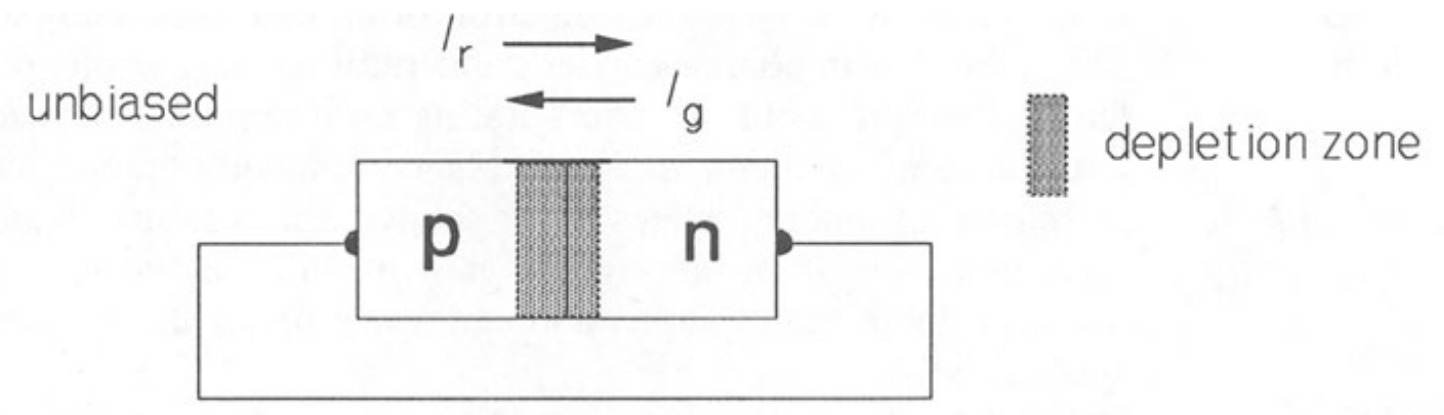
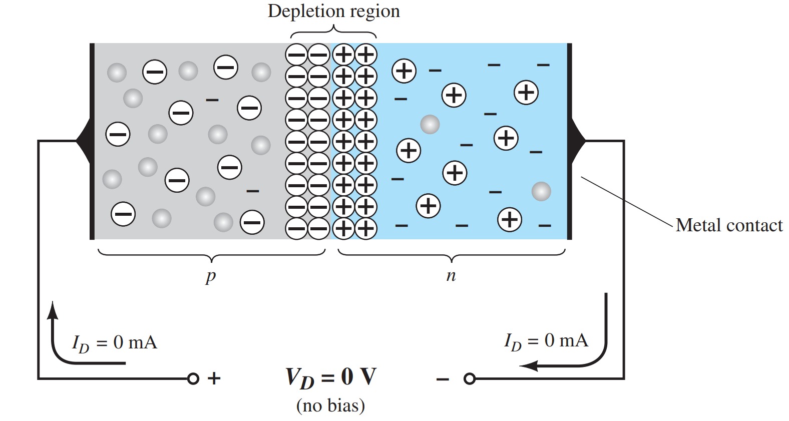
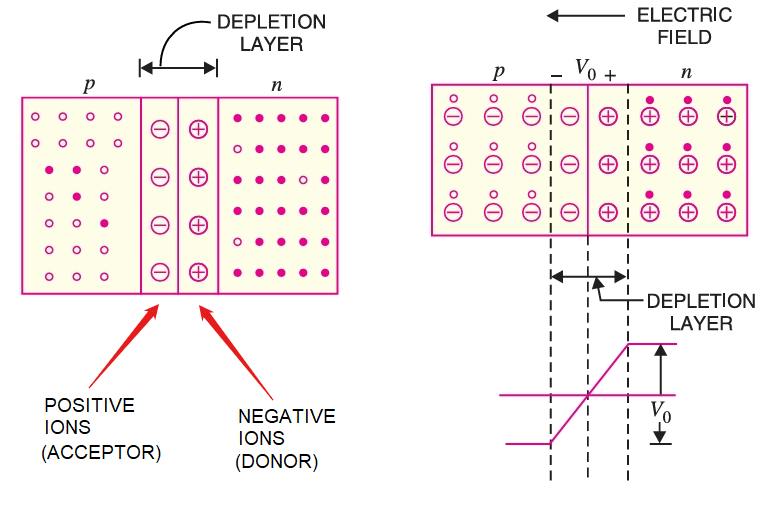
If leads are connected to the ends of each material, a two-terminal device results. Three options then become available: no bias, forward bias, and reverse bias. The term bias refers to applying an external voltage across the two terminals of the device to extract a response. The condition is the no-bias situation if no external voltage is applied.
The absence of a voltage across a resistor results in zero current through it.
Under no-bias conditions, any minority carriers (holes) in the \(n\)-type material that find themselves within the depletion region for any reason whatsoever will pass quickly into the \(p\)-type material. The closer the minority carrier is to the junction, the greater the attraction for the layer of negative ions and the less the opposition offered by the positive ions in the depletion region of the \(n\)-type material. The majority of carriers (electrons) of the \(n\)-type material must overcome the attractive forces of the layer of positive ions in the \(n\)-type material and the shield of negative ions in the \(p\)-type material to migrate into the area beyond the depletion region of the \(p\)-type material. However, the number of majority carriers is so large in the \(n\)-type material that there will invariably be a small number of majority carriers with sufficient kinetic energy to pass through the depletion region into the \(p\)-type material. Again, the same type of discussion can be applied to the majority carriers (holes) of the \(p\)-type material.
In the absence of an applied bias across a semiconductor diode, the net flow of charge in one direction is zero.
Reverse-Bias Condition
\(V_{D} \lt 0~V\)
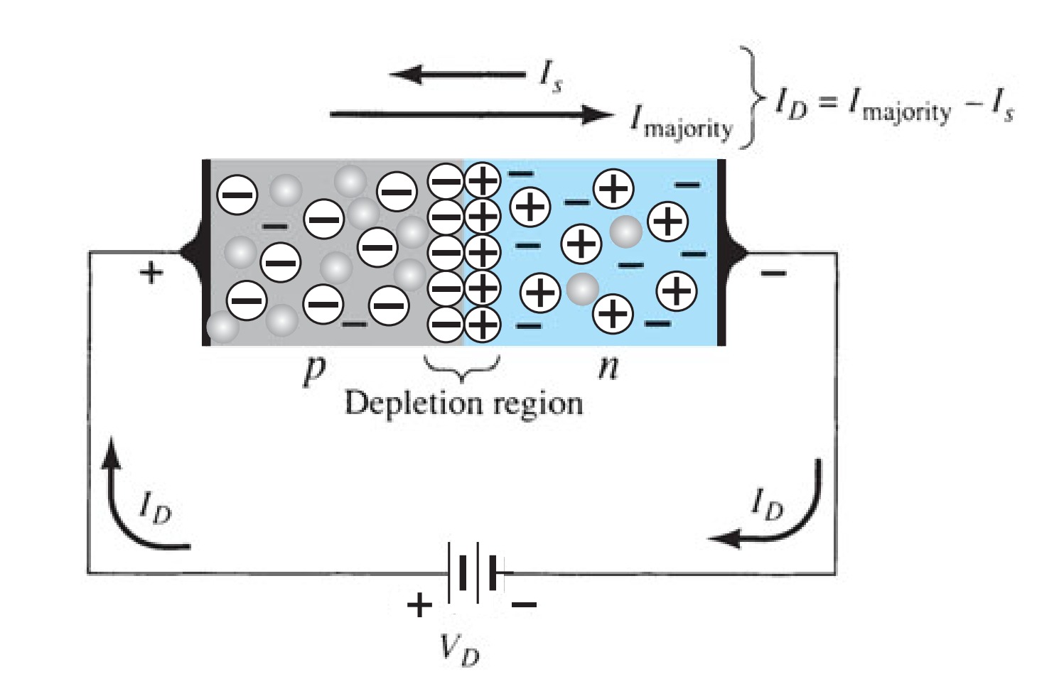
If an external potential of V volts is applied across the \(p-n\) junction such that the positive terminal is connected to the \(n\)-type material and the negative terminal is connected to the \(p\)-type material, as shown in the figure, the number of uncovered positive ions in the depletion region of the \(n\)-type material will increase due to the large number of free electrons drawn to the positive potential of the applied voltage. For similar reasons, the number of uncovered negative ions will increase in the \(p\)-type material. The net effect, therefore, is a widening of the depletion region. This widening of the depletion region will establish too great a barrier for the majority of carriers to overcome, effectively reducing the majority carrier flow to zero.
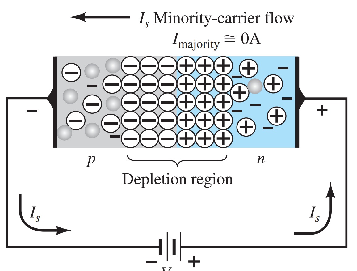
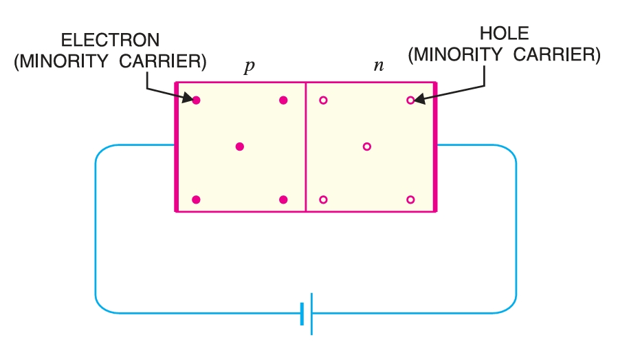
The number of minority carriers, however, entering the depletion region will not change, resulting in minority-carrier flow vectors of the same magnitude indicated in Fig. with no applied voltage.
The current that exists under reverse-bias conditions is called the reverse saturation current and is represented by \(I_{s}\).
The term saturation comes from the fact that it reaches its maximum level quickly and does not change significantly with increases in the reverse bias potential
Forward-Bias Condition
\(V_{D} \gt 0\) \(V\)
A forward bias or on condition is established by applying the positive potential to the \(p\)-type material and the negative potential to the \(n\)-type material, as shown in Fig.
The application of a forward-bias potential \(V_D\) will pressure electrons in the \(n\)-type material and holes in the \(p\)-type material to recombine with the ions near the boundary and reduce the width of the depletion region, as shown in Fig. The resulting minority-carrier flow of electrons from the \(p\)-type material to the \(n\)-type material (and of holes from the \(n\)-type material to the \(p\)-type material) has not changed in magnitude (since the conduction level is controlled primarily by the limited number of impurities in the material), but the reduction in the width of the depletion region has resulted in a heavy majority flow across the junction. An electron of the \(n\)-type material now sees a reduced barrier at the junction due to the reduced depletion region and a strong attraction for the positive potential applied to the \(p\)-type material. As the applied bias increases in magnitude, the depletion region will continue to decrease in width until a flood of electrons can pass through the junction, resulting in an exponential rise in current, as shown in the forward-bias region of the characteristics.
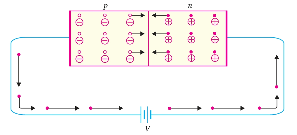
The mechanism of current flow in a forward biased \(pn\) junction can be summed up as under:
- (i) The free electrons from the negative terminal continue to pour into the \(n\)-region while the free electrons in the \(n\)-region move towards the junction.
- (ii) The electrons travel through the \(n\)-region as free-electrons i.e. current in \(n\)-region is by free electrons
- (iii) When these electrons reach the junction, they combine with holes and become valence electrons.
- (iv) The electrons travel through \(p\)-region as valence electrons i.e. current in the \(p\)-region is by holes.
- (v) When these valence electrons reach the left end of crystal, they flow into the positive terminal of the battery.
The current is carried by free electrons in \(n\)-type region whereas it is carried by holes in \(p\)-type region. However, the current is carried by free electrons in the external connecting wires.
Volt-Ampere Characteristics
Volt-ampere or \(V-I\) characteristic of a \(pn\) junction (also called a semiconductor diode) is the curve between voltage across the junction and the circuit current. Usually, voltage is taken along \(x\)-axis and current along \(y\)-axis. Fig. shows the circuit arrangement for determining the \(V-I\) characteristics of a \(pn\) junction. The characteristics can be studied under three heads, namely; zero external voltage, forward bias and reverse bias.
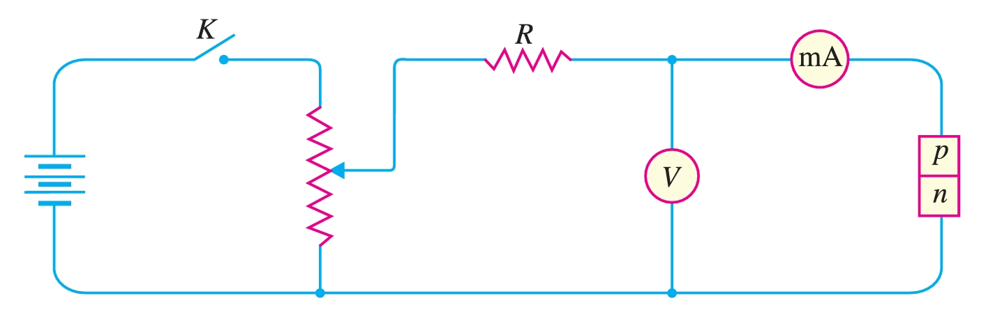
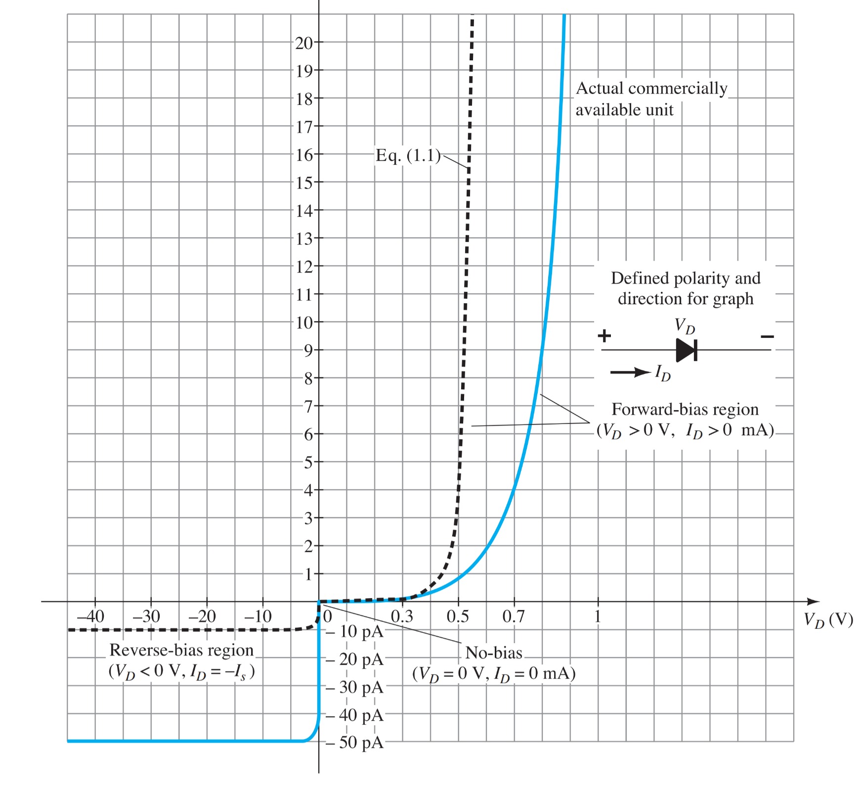
The general characteristics of a semiconductor diode can be defined by the following equation, referred to as Shockley’s equation, for the forward- and reverse-bias regions:
\[I_{D} = I_{s}(e^{V_{D}/\eta V_T} - 1)~(A)\]
where \(I_s\) is the reverse saturation current \(V_{D}\) is the applied forward-bias voltage across the diode \(\eta\) is an ideality factor, which is a function of the operating conditions and physical construction; it has a range between \(1\) and \(2\) depending on a wide variety of factors. The ideality factor, \( \eta=1\) for \(Ge\) and \(\eta=2\) for \(Si\) for relatively low levels of diode current (at or below the knee of the curve). The \( \eta=1\) for \(Ge\) and \(Si\) for higher levels of diode current (in the rapidly increasing section of the curve).
The voltage \(V_T\) in Eq. is called the thermal voltage and is determined by
\[V_T = \frac{k_B T_{K}}{q}~(V)\]
where \(k_B\) is Boltzmann's constant \(1.38 \times 10^{-23}\) \(J/K\)
\(T_K\) is the absolute temperature in kelvins \(273\) \(K\) the temperature in \(°C\)
\(q\) is the magnitude of electronic charge \(1.6 \times 10^{-19}\) \(C\)
If we expand the equation of each region:
\[I_{D} = I_{s}e^{V_{D}/\eta V_T} - I_{s}~~(A)\]
For positive values of \(V_{D}\), the first term of the above equation will grow very quickly and totally overpower the effect of the second term. The result is the following equation, which only has positive values and takes on the exponential format \(e^{x}\).
\[I_{D} = I_{s}(e^{V_{D}/\eta V_T})~~~[V_{D}~positive]\]
For negative values of \(V_D\), the exponential term drops very quickly below the level of \(I\), and the resulting equation for \(I_{D}\) is simply
\[I_{D} = -I_{s} ~~~[V_{D}~negative]\]
For negative values of \(V_{D}\), the current is essentially horizontal at the level of \(-I_{s}\).
The actual reverse saturation current of a commercially available diode will normally be measurably larger than that appearing as the reverse saturation current in Shockley’s equation.
This increase in level is due to a wide range of factors that include
- leakage currents
- generation of carriers in the depletion region
- higher doping levels that result in increased levels of reverse current
- sensitivity to the intrinsic level of carriers in the component materials by a squared factor—double the intrinsic level, and the contribution to the reverse current could increase by a factor of four.
- a direct relationship with the junction area—double the area of the junction and the contribution to the reverse current could double. High-power devices that have larger junction areas typically have much higher levels of reverse current.
- Temperature sensitivity—For every \(5\) \(°C\) increase in current, the level of reverse saturation current will double, whereas a \(10\) \(°C\) increase in current will result in a doubling of the actual reverse current of a diode.
Breakdown Region
Even though the scale of Fig. is in tens of volts in the negative region, there is a point where the application of too negative a voltage with the reverse polarity will result in a sharp change in the characteristics, as shown in Fig. The current increases at a very rapid rate in a direction opposite to that of the positive voltage region. The reverse bias potential that results in this dramatic change in characteristics is called the breakdown potential and is given the label \(V_{BV}\).
Avalanche breakdown
As the voltage across the diode increases in the reverse-bias region, the velocity of the minority carriers responsible for the reverse saturation current \(I_{s}\) will also increase. Eventually, their velocity and associated kinetic energy \((W_K= \frac{1}{2}mv^2)\) will be sufficient to release additional carriers through collisions with otherwise stable atomic structures. That is, an ionization process will result whereby valence electrons absorb sufficient energy to leave the parent atom. These additional carriers can then aid the ionization process to the point where a high avalanche current is established, and the avalanche breakdown region is determined.
Zener breakdown
The avalanche region \((V_{BV})\) can be brought closer to the vertical axis by increasing the doping levels in the \(p\)- and \(n\)-type materials. However, as \(V_{BV}\) decreases to very low levels, such as \(5\) \(V\), another mechanism, called Zener breakdown, will contribute to the sharp change in the characteristic. It occurs because there is a strong electric field in the region of the junction that can disrupt the bonding forces within the atom and “generate” carriers. Although the Zener breakdown mechanism is a significant contributor only at lower levels of \(V_{BV}\), this sharp change in the characteristic at any level is called the Zener region, and diodes employing this unique portion of the characteristic of a \(p–n\) junction are called Zener diodes.
The breakdown region of the semiconductor diode described must be avoided if the response of a system is not to be completely altered by the sharp change in characteristics in this reverse-voltage region. The maximum reverse-bias potential that can be applied before entering the breakdown region is called the peak inverse voltage (referred to simply as the \(PIV\) rating) or the peak reverse voltage (denoted the \(PRV\) rating).
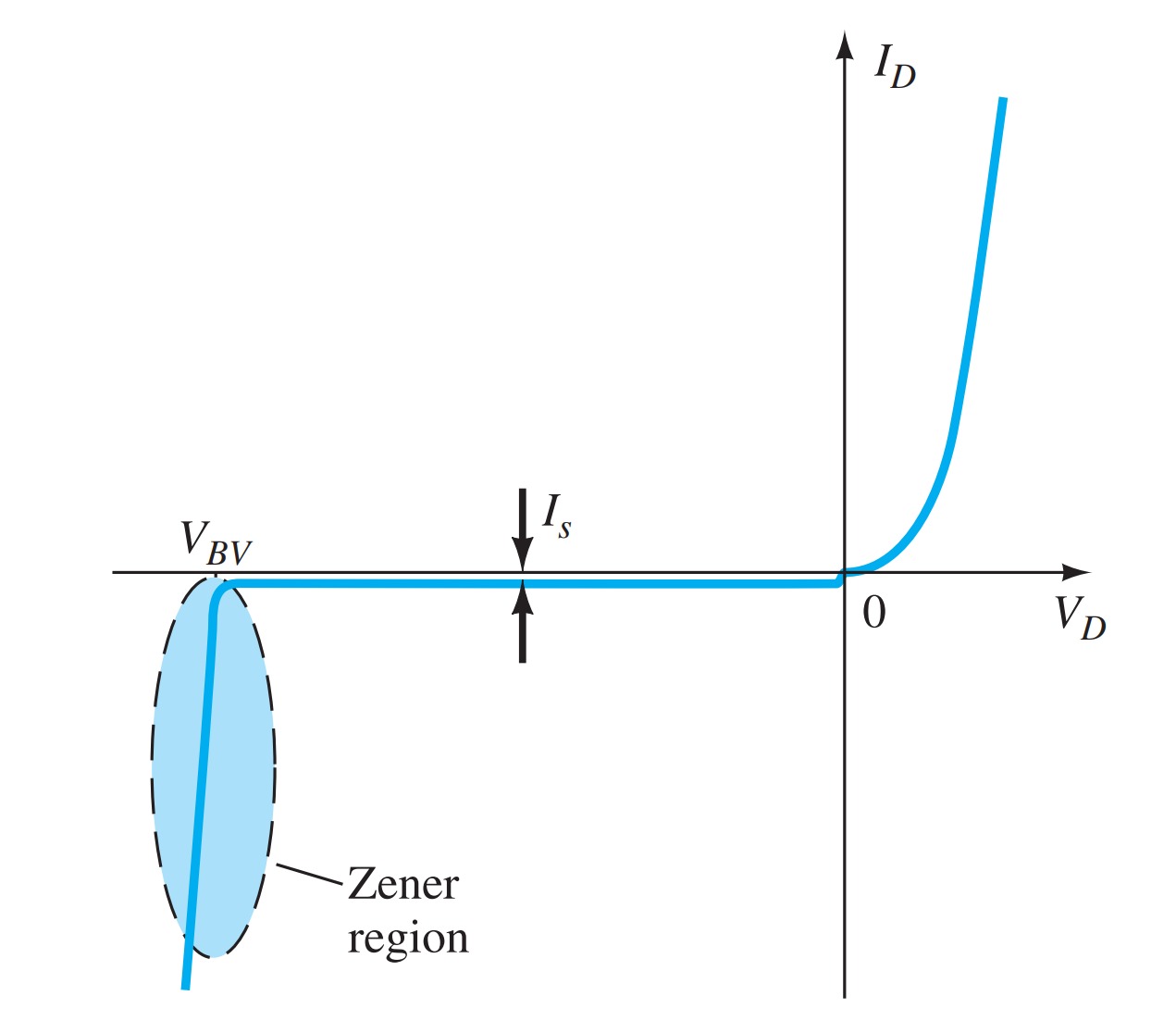
If an application requires a PIV rating more significant than that of a single unit, several diodes of the same characteristics can be connected in series. Diodes are also connected in parallel to increase the current-carrying capacity.
Temperature Effects
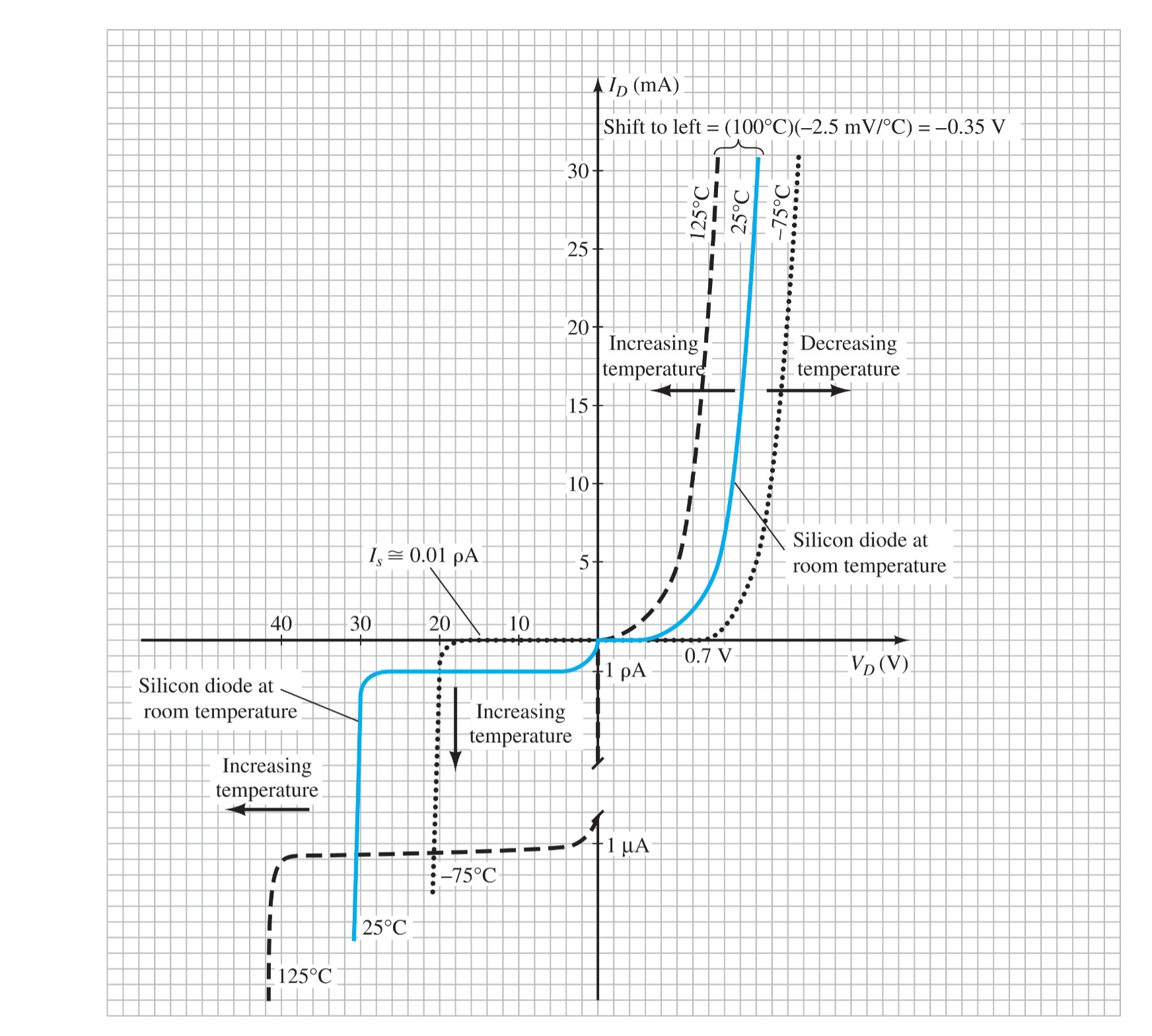
Temperature can have a marked effect on the characteristics of a semiconductor diode, as demonstrated by the characteristics of a silicon diode.
- In the forward-bias region, the characteristics of a silicon diode shift to the left at a rate of 2.5 mV per centigrade degree increase in temperature.
- In the reverse-bias region, the reverse current of a silicon diode doubles for every 10°C rise in temperature.
- The reverse breakdown voltage of a semiconductor diode will increase or decrease with temperature.
Silicon versus Germanium
Silicon diodes have, in general, higher PIV and current rating and wider temperature ranges than germanium diodes. PIV ratings for silicon can be in the neighborhood of 1000 V, whereas the maximum value for germanium is closer to 400 V. Silicon can be used for applications in which the temperature may rise to about 200°C (400°F), whereas germanium has a much lower maximum rating (100°C). The disadvantage of silicon as compared to germanium, as is the higher forward-bias voltage required to reach the region of upward swing. It is typically of the order of magnitude of 0.7 V for commercially available silicon diodes and 0.3 V for germanium diodes when rounded off to the nearest tenths. The increased offset for silicon is due primarily to the \(\eta\) factor. This factor plays a part in determining the shape of the curve only at very low current levels. Once the curve starts its vertical rise, the \(\eta\) factor drops to 1 (the continuous value for germanium). This is evidenced by the similarities in the curves once the offset potential is reached.
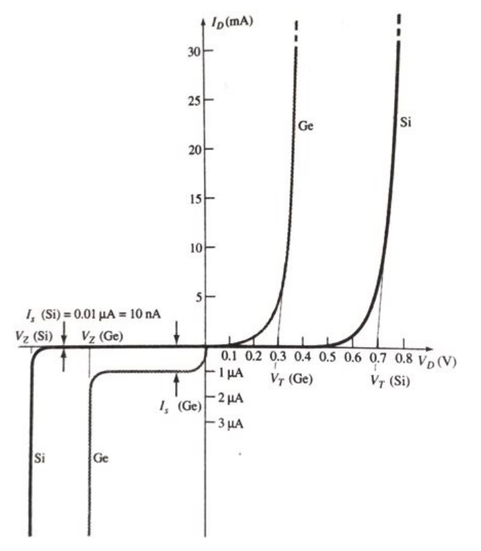
The threshold potential for Silicon (Si) and Germanium (Ge) is
\[V_{T} = 0.7 ~\text{Volts} ~(\text{Si})\] \[V_{T} = 0.3 ~\text{Volts} ~(\text{Ge})\]
Typical values of saturation current, \(I_{s}\) for silicon are much lower than that of germanium for similar power and current levels and even at high temperatures the levels of \(I_{s}\) for silicon diodes do not reach the same high levels obtained for germanium.
Limitations of pn junction
Every \(p-n\) junction has limiting values of maximum forward current, peak inverse voltage and maximum power rating. The \(p-n\) junction will give satisfactory performance if it is operated within these limiting values. However, if these values are exceeded, the \(p-n\) junction may be destroyed due to excessive heat.
(i) Maximum forward current
Maximum forward current is the highest instantaneous forward current that a \(p-n\) junction can conduct without damage to the junction. Manufacturer’s data sheet usually specifies this rating. If the forward current in a \(p-n\) junction is more than this rating, the junction will be destroyed due to overheating.
(ii) Peak inverse voltage (PIV)
Peak inverse voltage is the maximum reverse voltage that can be applied to the \(p-n\) junction without damage to the junction. If the reverse voltage across the junction exceeds its PIV, the junction may be destroyed due to excessive heat. The peak inverse voltage is of particular importance in rectifier service. A \(p-n\) junction diode is used as a rectifier to change alternating current into direct current. In such applications, the reverse voltage across the diode during negative half-cycle of a.c. does not exceed the PIV of diode.
(iii) Maximum power rating
Maximum power rating is the maximum power that can be dissipated at the junction without damaging it. The power dissipated at the junction is equal to the product of junction current and the voltage across the junction. This is a very important consideration and is invariably specified by the manufacturer in the data sheet.
Diode Resistance
The resistance of the diode will also change due to the nonlinear shape of the characteristic curve as the operating point of a diode moves from one region to another. A forward-biased diode conducts easily, whereas a reverse-biased diode practically conducts no current. This means that the forward resistance of a diode is much lower than its reverse resistance.
Forward resistance.
The resistance offered by the diode to forward bias is known as forward resistance. This resistance is not the same for the flow of direct current as for the alternating current. Accordingly, this resistance is of two types, namely, d.c. forward resistance (Static Resistance) and a.c. forward resistance (Dynamic Impedance).
Static Resistance (D.C. Resistance)
Applying a DC voltage to a circuit containing a semiconductor diode results in an operating point on the characteristic curve that remains constant over time. The resistance of the diode at the operating point can be found simply by finding the corresponding levels of \(V_D\) and \(I_D\) as shown in Fig. 1, and applying the following equation:
\[R_{D} = \frac{V_{D}}{I_{D}}\]
The dc resistance levels at the knee and below will be greater than the resistance levels obtained for the vertical rise section of the characteristics, i.e., the lower the current through a diode, the higher the dc resistance level. The DC resistance of a diode is independent of the shape of the characteristic in the region surrounding the point of interest.
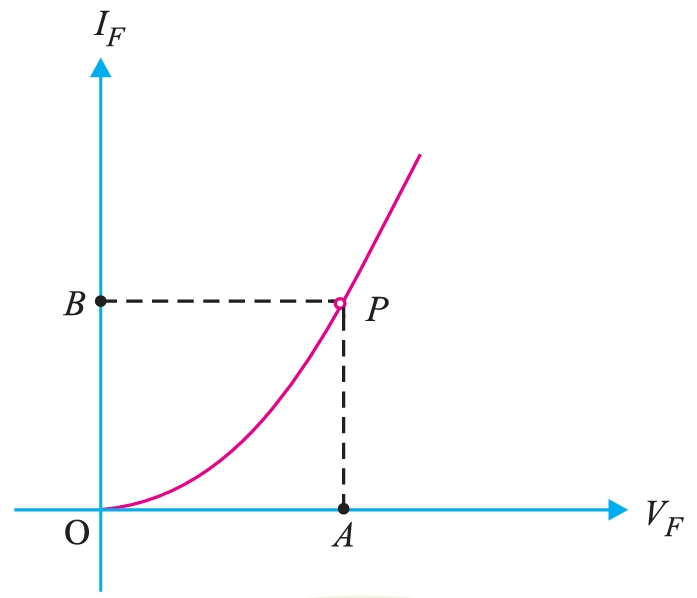
The DC resistance levels for the diode
| \(V_{D}\) | \(I_{D}\) | \(R_{D}\) |
|---|---|---|
| 0.5 V | 2 \(mA\) | 250 \(\Omega\) |
| 0.8 V | 20 \(mA\) | 40 \(\Omega\) |
| 10 V | 1 \(\mu A\) | 10 \(M\Omega\) |
Dynamic Resistance (A.C. Impedance)
A sinusoidal voltage applied to the input varies the input and moves the instantaneous operating point up and down along the characteristics, thus defining a specific change in current and voltage; hence, the resistance also changes accordingly.
A straight line drawn tangent to the curve through the \(Q\)-point as shown in Fig. 2 will define a particular change in voltage and current that can be used to determine the acor dynamic resistance for this region of the diode characteristics. An effort should be made to keep the change in voltage and current as small as possible and to keep them equidistant from the Q-point. In equation form,
\[r_{d} = \frac{\Delta V_{d}}{I_{d}}\]
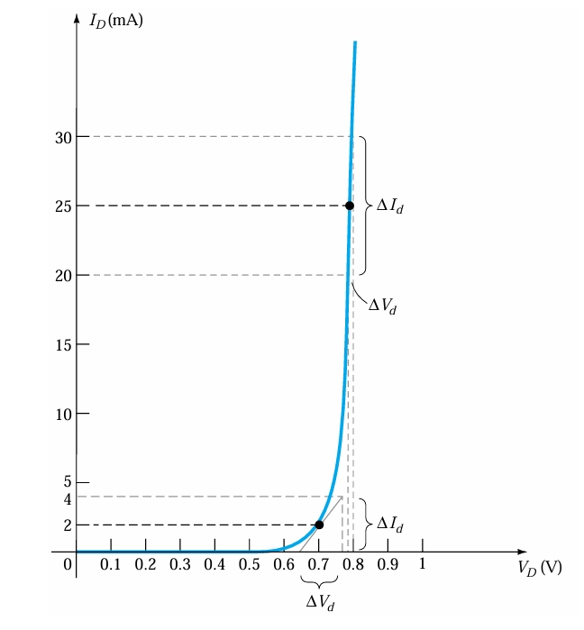
The steeper the slope, the less the value of \(V_{d}\) for the same change in \(I_{d}\) and the less the resistance. The ac resistance in the vertical-rise region of the characteristic is therefore quite small, while the ac resistance is much higher at low current levels.
The dynamic resistance levels for the diode
| \(V_{1}\) | \(V_{2}\) | \(I_{1}\) | \(I_{2}\) | \(V_{d}\) | \(I_{d}\) | \(r_{d}\) | \(R_{D} = \frac{V_{1}+V_{1}}{I_{1}+I_{2}}\) |
|---|---|---|---|---|---|---|---|
| 0.65 V | 0.75 V | 0 \(mA\) | 4 \(mA\) | 0.11 V | 4 \(mA\) | 27.5 \(\Omega\) | 350 \(\Omega\) |
| .78 V | 0.80 V | 20 \(mA\) | 30 \(mA\) | 0.02 V | 10 \(mA\) | 2 \(\Omega\) | 31.62 \(\Omega\) |
The dynamic resistance is defined as the The derivative of a function at a point is equal to the slope of the tangent line drawn at that point.
We can derive the dynamic resistance from the diode equation as follows:
\[I_D = [I_s (e^{(\eta V_D/V_T)}-1)]\]
Taking the derivative of the above equation with respect to the applied bias (\(V_D\)) will result in
\[\frac{d}{d V_D}(I_D) = \frac{d}{d V}[I_s (e^{(\eta V_D/V_T)}-1)]\]
\[\frac{d I_D}{d V_D} = I_s e^{(\eta V_D/V_T)}\left(\frac{\eta}{V_T}\right)\] \[ \frac{d I_D}{d V_D} = \frac{\eta}{V_T}(I_D + I_s)\]
But, \(I_D \gg I_s\) in the forward characteristic of a \(p-n\) junction diode, hence, we can ignore \(I_s\), and the equation becomes
\[\frac{d I_D}{d V_D} \cong \left(\frac{\eta}{V_T}\right) I_D \]
Substituting \(\eta = 1\) for \(Ge\) and \(Si\) in the vertical-rise section of the forward characteristics, we get, \(V_T\) as
\[V_T = \frac{k_B T}{e} = \frac{1.38 \times 10^{-23} \times T}{1.6 \times 10^{-19}} = \left(\frac{T}{11600}\right)\]
Hence,
\[\frac{d I_D}{d V_D} = \left(\frac{11600}{T}\right) I_D \]
and at room temperature, 298 K, we get,
\[\frac{d I_D}{d V_D} = \left(\frac{11600}{298}\right) I_D \cong 38.93 ~I_D\]
Then the dynamic resistance is obtained by taking the inverse of the above equation, so we get
\[r_d = \frac{d V_D}{d I_D} = \frac{1}{38.93 ~I_D} \]
or
\[r_d = \frac{26 ~mV}{I_D}\bigg|_{\text{Ge, Si}}\]
It implies that the dynamic resistance can be found simply by substituting the operating current of the diode into the equation. For lesser values of \(I_{D}\), \(\eta = 2\), and the value of \(r_d\) obtained must be multiplied by a factor of 2. For small values of \(I_{D}\) below the knee of the curve, the above equation of dynamic resistance becomes inappropriate.
All the resistance levels determined thus far have been defined by the \(p-n\) junction and do not include the resistance of the semiconductor material itself (called body resistance) and the resistance introduced by the connection between the semiconductor material and the external metallic conductor (called contact resistance). These additional resistance levels can be included in \(r_d\) by adding resistance denoted by \(r_B\). The resistance \(r_d\), therefore, includes the dynamic resistance and the resistance \(r_B\).
\[r'_d = \left[\frac{26 ~mV}{I_D}\right] + r_B ~~~\Omega\]
Average AC resistance
If the input signal is sufficiently large to produce a broad swing (Figure 3), the resistance associated with the device for this region is called the average ac resistance. The average ac resistance is, by definition, the resistance determined by a straight line drawn between the two intersections established by the maximum and minimum values of input voltage
\[r_{av} = \frac{d V_D}{d I_D}\bigg|_{\text{point to point}} \]
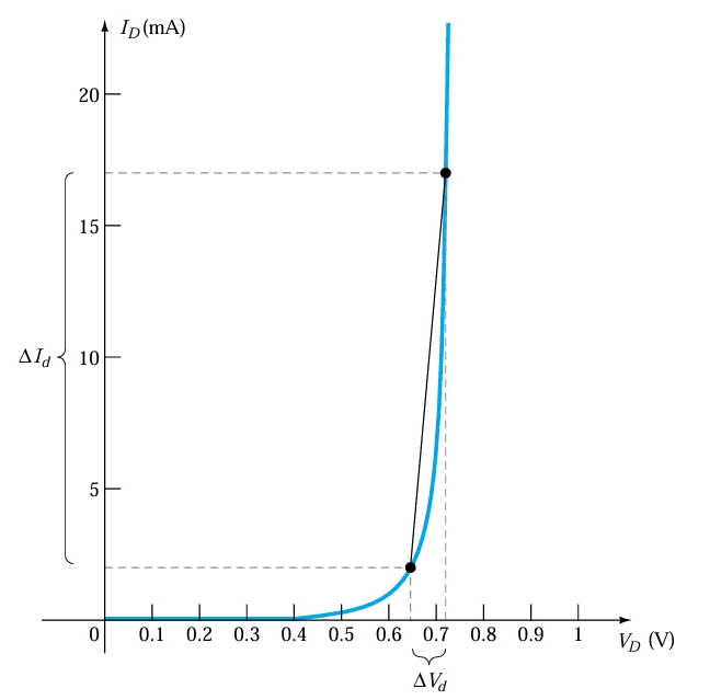
Reverse resistance.
The resistance offered by the diode to the reverse bias is known as reverse resistance. The resistance levels in the reverse-bias region will naturally be quite high. It can be d.c. reverse resistance or a.c. reverse resistance depending on whether the reverse bias is direct or changing. Ideally, the reverse resistance of a diode is infinite. However, in practice, the reverse resistance is not infinite because for any value of reverse bias, there does exist a small leakage current. It may be emphasised that reverse resistance is much larger than forward resistance. In germanium diodes, the ratio of reverse to forward resistance is 40000 : 1, while for silicon, this ratio is 1000000 : 1.