Diode equivalent circuits
An equivalent circuit is a combination of elements properly chosen to best represent the actual terminal characteristics of a device, system, or such in a particular operating region.
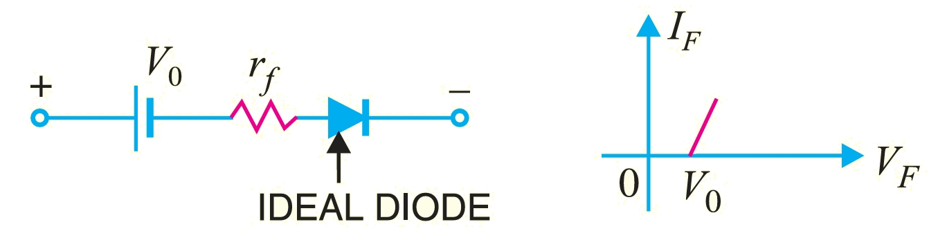
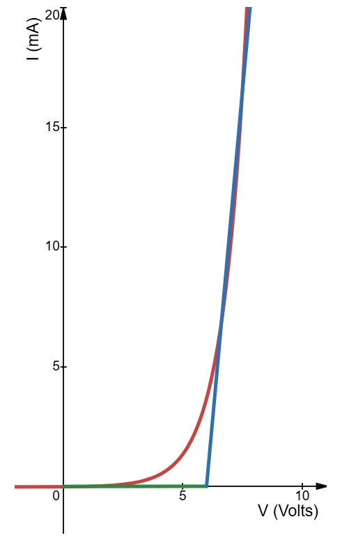
Piecewise-Linear Equivalent Circuit
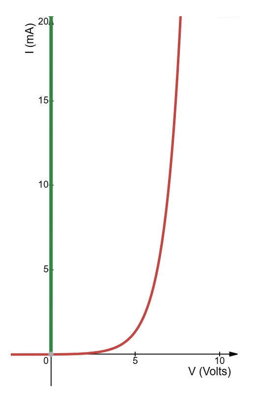
An equivalent circuit for a diode is to approximate the characteristics of the device by straight-line segments, and the resulting segments are sufficiently close to the actual curve to establish an equivalent circuit that will provide an excellent first approximation to the actual behavior of the device. It defines the resistance level of the device when it is in the ON state. The ideal diode is included to ensure that conduction occurs in only one direction through the device, and that a reverse-bias condition results in the device being in an open-circuit state. Since a silicon semiconductor diode does not reach the conduction state until \(V_D\) reaches 0.7 V with a forward bias, a battery \(V_T\) opposing the conduction direction must appear in the equivalent circuit. The battery simply specifies that the voltage across the device must be greater than the threshold battery voltage before conduction through the device in the direction dictated by the ideal diode can be established. When conduction is established, the resistance of the diode will be the specified value of \(r_{av}\).
Simplified Equivalent Circuit
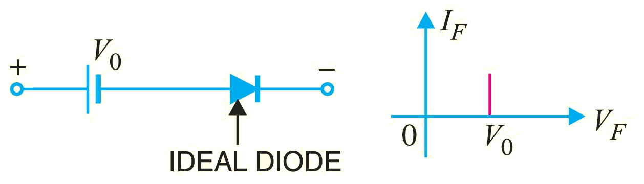
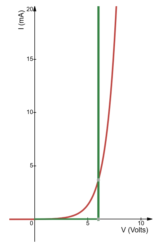
For most applications, the resistance \(r_{av}\) is sufficiently small to be ignored in comparison to the other elements of the network.
\[R_{network} \gg r_{av}\]
The removal of \(r_{av}\) from the equivalent circuit is the same as implying that the characteristics of the diode. It states that a forward-biased silicon diode is used in an electronic system. Under DC conditions, it has a drop of 0.7 V across it in the conduction state at any diode current level.
Ideal Equivalent Circuit
Now that \(r_{av}\) has been removed from the equivalent circuit, it is established that a 0.7 V level can often be ignored in comparison to the applied voltage level. In this case, the equivalent circuit reduces to that of an ideal diode.
\[R_{network} \gg r_{av} \]
\[E_{network} \gg V_T\]
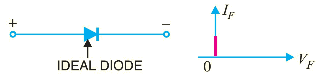
Diode Clippers
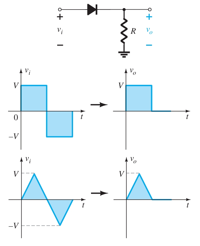
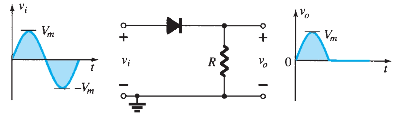
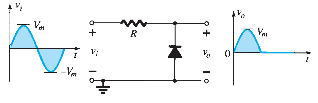
There are a variety of diode networks called clippers that have the ability to clip off a portion of the input signal without distorting the remaining part of the alternating waveform. Depending on the orientation of the diode, the positive or negative region of the input signal is clipped off.
Clippers are networks that employ diodes to clip away a portion of an input signal without distorting the remaining part of the applied waveform.
There are two general categories of clippers: series and parallel. In the series configuration, the diode is in series with the load, whereas in the parallel configuration, the diode is in a branch parallel to the load.
Series Clipper
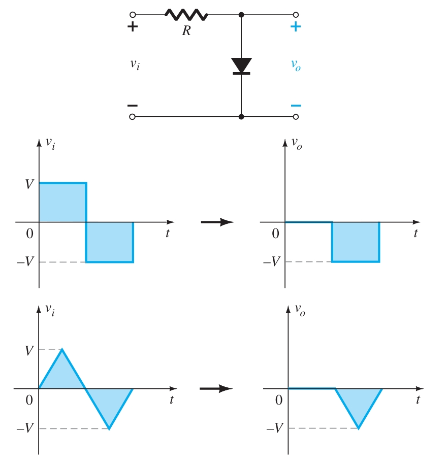
The response of the series configuration to a variety of alternating waveforms is provided in Fig. 1. Although first introduced as a half-wave rectifier (for sinusoidal waveforms), there are no boundaries on the type of signals that can be applied to a clipper.
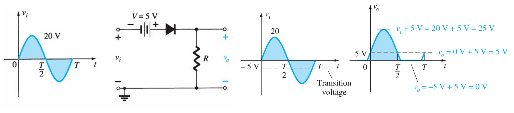
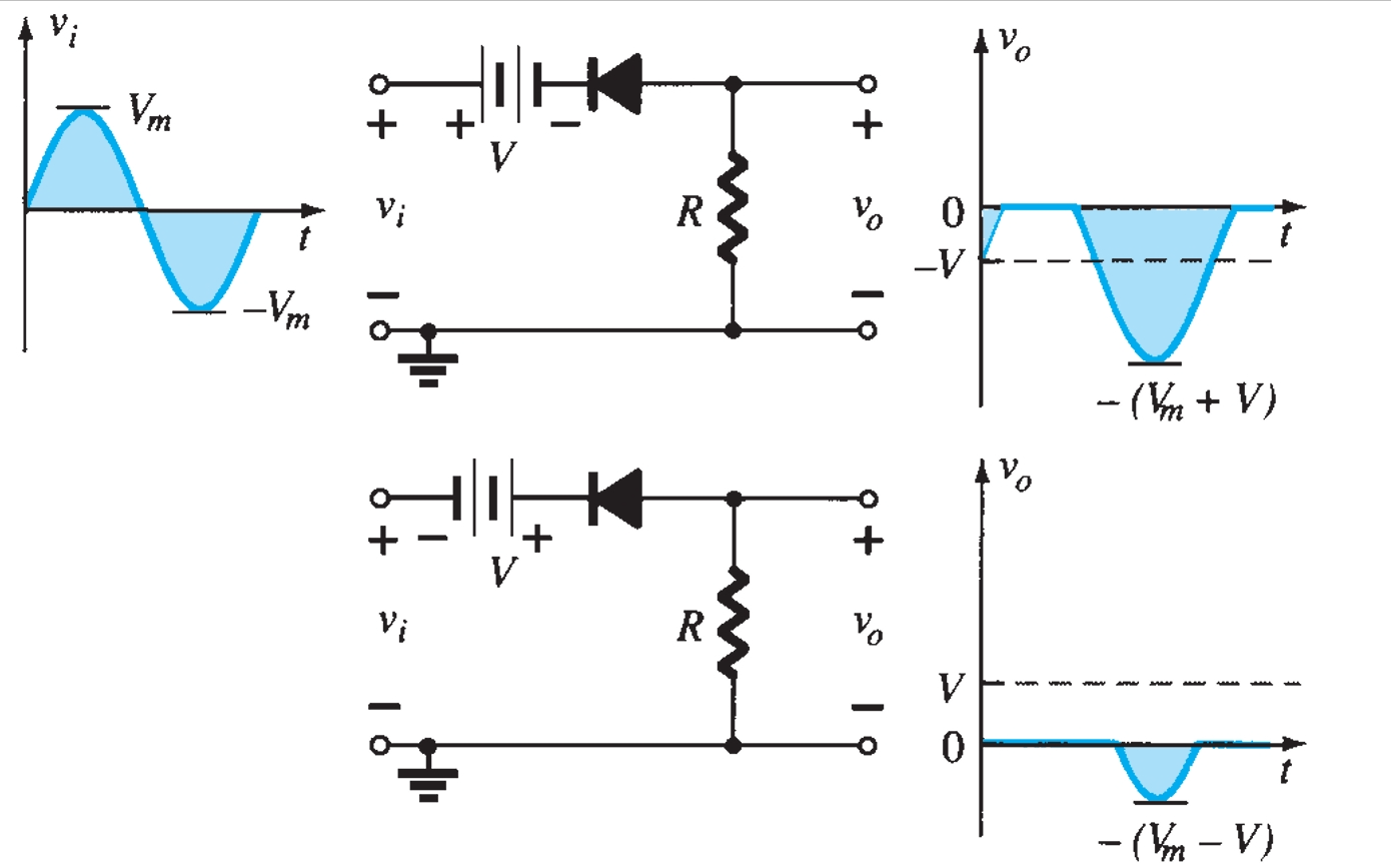
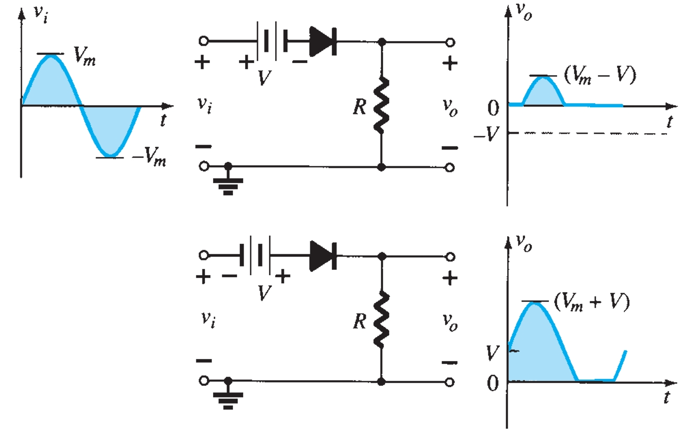
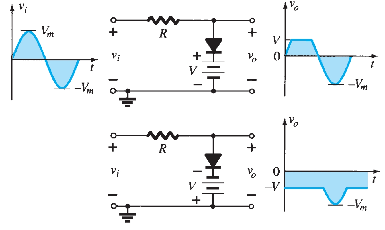
The addition of a DC supply, such as shown in Fig. 2, can have a pronounced effect on the output of a clipper. For the network of Fig. 1, the direction of the diode suggests that the signal \(v_i\) must be positive to turn it on. The DC supply further requires that the voltage \(v_i\) be greater than \(V\) volts to turn the diode on. The negative region of the input signal is pressuring the diode into the off state, which is further supported by the DC supply. In general, therefore, we can be quite sure that the diode is an open circuit (off state) for the negative region of the input signal. For an input voltage greater than \(V\) volts, the diode is in the short-circuit state, while for input voltages less than \(V\) volts, it is in the open-circuit or off state. When the diode is in the short-circuit state, the output voltage vo can be determined by :
\[v_o = v_i - V\]
An instantaneous value of \(v_i\), the input, can be treated as a DC supply of that value, and the corresponding DC value (the instantaneous value) of the output can be determined.
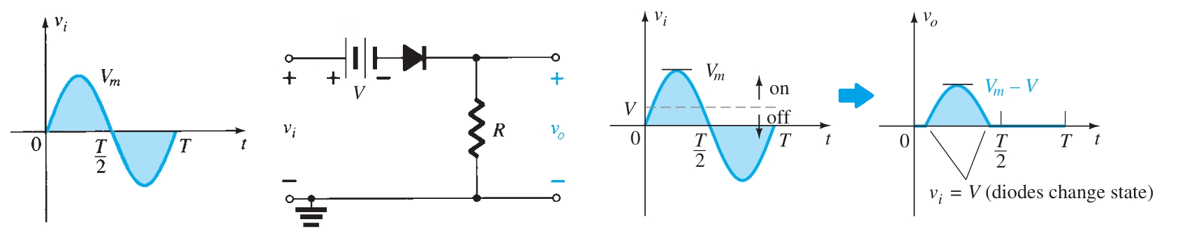
For instance, at \(v_i = V_m\), the network to be analyzed is as shown in Fig. 2. For \(V_m > V\), the diode is in the short-circuit state, and \(vo\) is as shown in Fig. 3.
\[v_o = V_m - V\]
At \(v_i = V\) the diodes change state; at \(v_i = -V_m\), \(v_o = 0~V\) and the complete curve for \(vo\) can be sketched as shown in Fig. 3.
Parallel Clipper
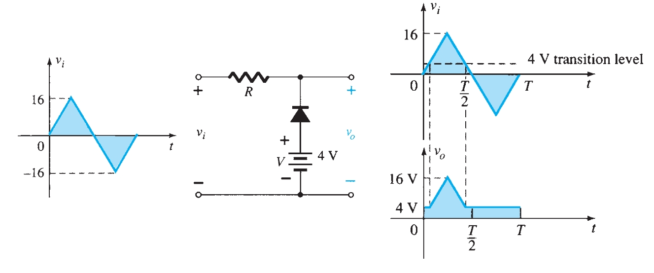
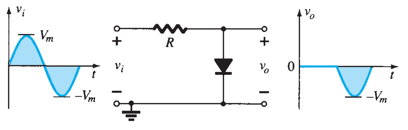
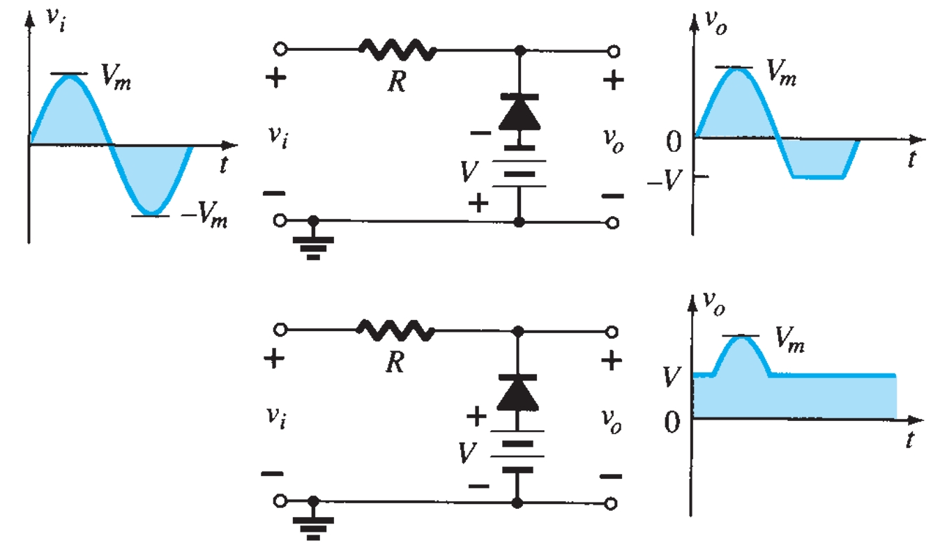
The network in Fig. 4 is the simplest parallel diode configuration, with the same output for any given input. The analysis of parallel configurations is very similar to that applied to series configurations. The polarity of the DC supply and the direction of the diode strongly suggest that the diode will be in the on state for the negative region of the input signal. For this region, the network has the diode short-circuited (on), where the defined terminals for \(v_o\) require that \(v_o = V = 4 ~V\).
Since the DC supply is obviously pressuring the diode to stay in the short circuit state, the input voltage must be greater than \(4 ~V\) for the diode to be in the off state. Any input voltage less than \(4 ~V\) will result in a short-circuited diode.
In the open-circuit state, the network has the diode in the off state, so \(v_o = v_i\). Completing the sketch of \(v_o\) results in the waveform of Fig. 4.
Clipper Circuits
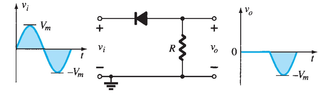
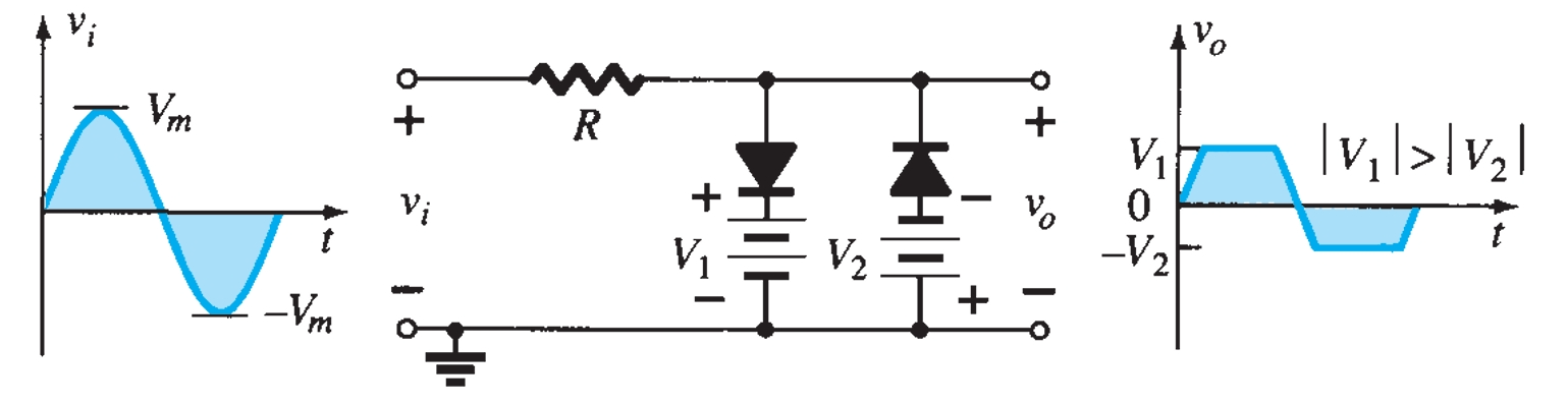
Various configurations of output waveforms are obtained using the combination of series and parallel clippers, which are given below:
Diode Rectifier Circuits
The electric power available is usually an a.c. supply for reasons associated with the economics of generation and transmission. The supply voltage varies sinusoidally and has a frequency of 50 Hz. It is used for lighting, heating, and electric motors. But there are many applications (e.g., electronic circuits) where d.c. supply is needed. When such a d.c. supply is required, the mains a.c. Supply is rectified by using crystal diodes. The following two rectifier circuits can be used : (i) Half-wave rectifier, (ii) Full-wave rectifier.
Half-Wave Rectifier
In half-wave rectification, the rectifier conducts current only during the positive half-cycles of the input a.c. supply. The negative half-cycles of a.c. supply is suppressed, i.e., during negative half-cycles, no current is conducted, and hence no voltage appears across the load. Therefore, current always flows in one direction (i.e., d.c.) through the load, alternating every half-cycle.
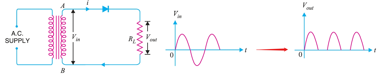
Fig. 14 shows the circuit where a \(p-n\) junction diode acts as a half-wave rectifier. The a.c. supply to be rectified is applied in series with the diode and load resistance \(R_{L}\). Generally, a.c. supply is given through a transformer. The use of a transformer permits two advantages. Firstly, it allows us to step up or step down the a.c. input voltage as the situation demands. Secondly, the transformer isolates the rectifier circuit from the power line, thereby reducing the risk of electric shock.
The a.c. voltage across the secondary winding AB changes polarity after every half-cycle. During the positive half-cycle of input a.c. voltage, end \(A\) becomes positive w.r.t. end \(B\). This makes the diode forward-biased, and hence it conducts current. During the negative half-cycle, end \(A\) is negative w.r.t. end \(B\). Under this condition, the diode is reverse-biased biased and it conducts no current. Therefore, current flows through the diode during the positive half-cycles of the input a.c. voltage only; it is blocked during the negative half-cycles. In this way, current through the load \(R_{L}\) always flows in the same direction. Hence d.c. output is obtained across \(R_{L}\). It may be noted that output across the load is pulsating d.c. These pulses are known as ripple voltage. The output frequency of a half-wave rectifier is equal to the input frequency (50 Hz).
Advantages
The main advantages of a half-wave rectifier are :
- (i) Requires only one diode for operation, making the circuit very simple and so it is economical.
- (ii) It is easy to construct, compact and lightweight and easy to understand.
- (iii) Useful for low-power applications
Disadvantages
The main disadvantages of a half-wave rectifier are :
- (i) The pulsating current in the load contains an alternating component whose basic frequency is equal to the supply frequency. Therefore, an elaborate filtering is required to produce a steady direct current.
- (ii) The a.c. supply delivers power only half the time. Therefore, the output is low.
Efficiency of Half-Wave Rectifier
The ratio of d.c. power output to the applied input a.c. power is known as rectifier efficiency, i.e.
\[\text{Rectifier efficiency, } \eta = \frac{\text{d.c. power output}}{\text{Input a.c. power}}\]
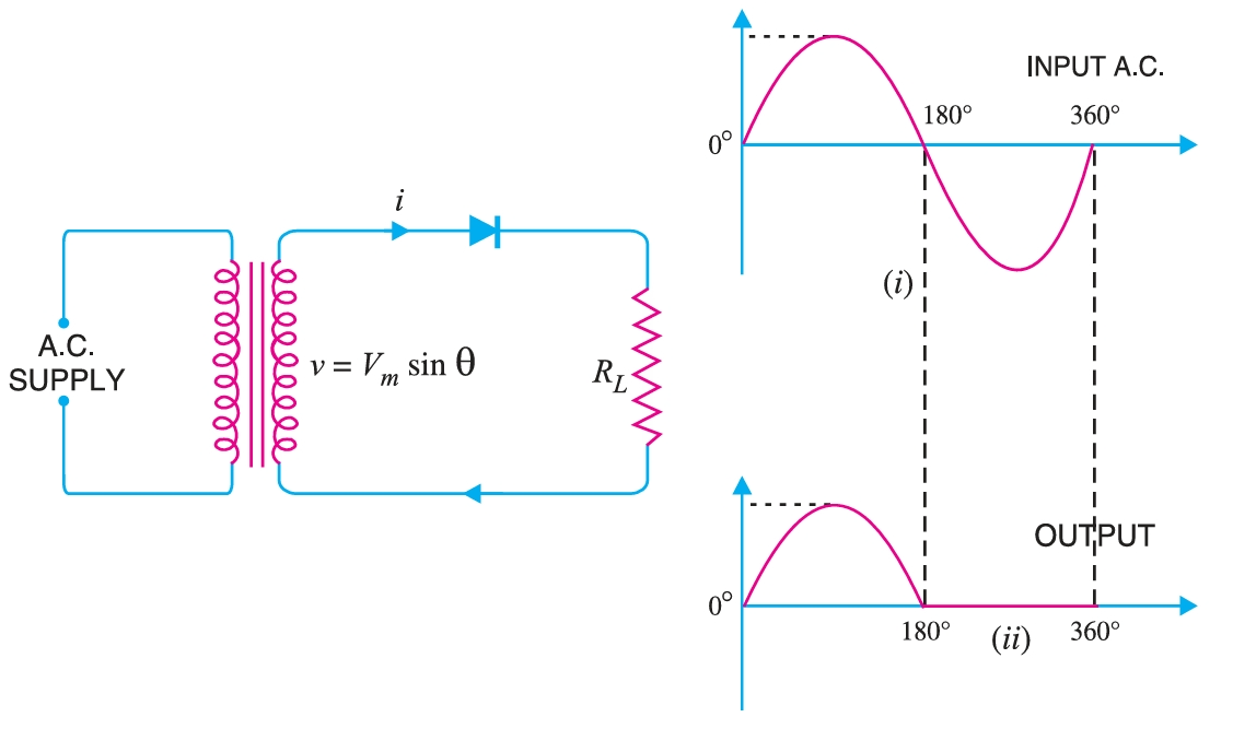
Consider a half-wave rectifier shown in Fig 15. The alternating voltage and current that appears across the secondary winding is given as:
\[V(\theta) = V_{m} \sin \theta \\ i(\theta) = I_{m} \sin \theta\]
where
\[I_m =\frac{V_m}{(r_d+R_L)}\]
Let \(r_{d}\) and \(R_{L}\) be the diode resistance and load resistance, respectively. The diode conducts during the positive half-cycles of a.c. supply while no current flows during the negative half-cycles.
- d.c. power The output current is a pulsating direct current. Therefore, in order to find d.c. power, the average current must be determined. \[I_{av} = I_{dc} = \frac{1}{2\pi} \int_0^{2\pi} i ~d\theta = \frac{1}{2\pi} \int_0^{2\pi} \frac{V_m}{(r_d+R_L)} \sin\theta ~d\theta\] \[I_{dc} = \frac{1}{2\pi} \left[\int_0^{\pi} \frac{V_m}{(r_d+R_L)} \sin\theta ~d\theta + \int_{\pi}^{2\pi} \frac{0}{(r_d+R_L)} \sin\theta ~d\theta \right] \] \[I_{dc} = \frac{1}{2\pi} \left[\int_0^{\pi} \frac{V_m}{(r_d+R_L)} \sin\theta ~d\theta + 0 \right] \] \[I_{dc} = \frac{V_m}{2\pi(r_d+R_L)} \int_0^{\pi} \sin\theta ~d\theta \] \[I_{dc} = \frac{V_m}{2\pi(r_d+R_L)}[-\cos\theta]_0^\pi \] \[I_{dc} = \frac{V_m}{2\pi(r_d+R_L)} \times 2 = \frac{V_m}{(r_d+R_L)}\frac{1}{\pi}\] \[I_{dc} = \frac{I_m}{\pi} \] \[\text{d.c. power, } P_{dc} = I_{dc}^2 R_{L}\] \[P_{dc} = \left(\frac{I_m}{\pi}\right)^2 R_{L}\]
- a.c. power input The current through the half wave rectifier circuit, \(I_{rms}\) is given as: \[I_{rms} = \sqrt{\frac{1}{2\pi} \int_0^{\pi} i^2 ~d\theta}\] \[I_{rms} = \sqrt{\frac{1}{2\pi} \int_0^{\pi} I_{m}^2 \sin^{2}\theta ~d\theta}\] \[I_{rms} = \sqrt{\frac{I_{m}^2}{2\pi} \int_0^{\pi} \sin^{2}\theta ~d\theta}\] \[I_{rms} = \sqrt{\frac{I_{m}^2}{2\pi} \int_0^{\pi} \sin^{2}\theta ~d\theta}\] \[I_{rms} = \sqrt{\frac{I_{m}^2}{2\pi} \int_0^{\pi} \left(\frac{1 - \cos~2\theta}{2}\right) ~d\theta}\] \[I_{rms} = \sqrt{\frac{I_{m}^2}{2\pi} \left[ \frac{\theta}{2} - \frac{1}{4}\sin~2\theta \right]_0^{\pi}}\] \[I_{rms} = \sqrt{\frac{I_{m}^2}{2\pi} \left[ \frac{\pi}{2} - \frac{1}{4}\sin(2\pi) \right]}\] \[I_{rms} = \sqrt{\frac{I_{m}^2}{2\pi} \left[ \frac{\pi}{2} \right]}\] \[I_{rms} = \sqrt{\frac{I_{m}^2}{4}}\] \[I_{rms} = \frac{I_{m}}{2}\] The a.c. power input is given by : \[\text{a.c. power, } P_{ac} = I_{rms}^2 (r_d+R_{L})\] For half wave rectified wave, \(I_{rms} = \left(\frac{I_m}{2}\right)\) \[\therefore\qquad P_{ac} = \left(\frac{I_m}{2}\right)^2 (r_d+R_{L})\]
- Rectifier efficiency \[\therefore \qquad \text{Rectifier efficiency} = \frac{\text{d.c. output power}}{\text{a.c. input power}}\] \[\eta= \frac{\left(\frac{I_m}{\pi}\right)^2 R_{L}}{\left(\frac{I_m}{2}\right)^2(r_d+R_{L})}\] \[\eta = \frac{4}{\pi^2} \left[\frac{R_{L}}{(r_d+R_{L})}\right] = 0.406~\left[\frac{R_{L}}{(r_d+R_{L})}\right]\] \[\eta = \frac{0.406}{\left(1+\frac{r_d}{R_{L}}\right)}\]
The efficiency will be maximum if \(r_d\) is negligible as compared to \(R_{L}\).
\[\therefore\qquad \qquad \text{Max. rectifier efficiency} = 40.6 \%\] This shows that in half-wave rectification, a maximum of \(40.6 \%\) of a.c. power is converted into d.c. power.
Full-Wave Rectifier
In full-wave rectification, current flows through the load in the same direction for both half-cycles of input a.c. voltage. This can be achieved using two diodes that alternate. For the positive half-cycle of the input voltage, one diode supplies current to the load, and for the negative half-cycle, the other diode does so; current is always in the same direction through the load. Therefore, a full-wave rectifier utilises both half-cycles of input a.c. voltage to produce the d.c. output. The following two circuits are commonly used for full-wave rectification : (i) Centre-tap full-wave rectifier, (ii) Full-wave bridge rectifier
Centre-Tap Full-Wave Rectifier
The circuit employs two diodes, \(D1\) and \(D2\), as shown in Fig. 16. A centre-tapped secondary winding \(AB\) is used with two diodes connected so that each uses one half-cycle of input a.c. voltage. In otherwords, diode \(D1\) utilises the a.c. voltage appearing across the upper half (\(OA\)) of the secondary winding for rectification, while diode \(D2\) uses the lower half winding \(OB\).
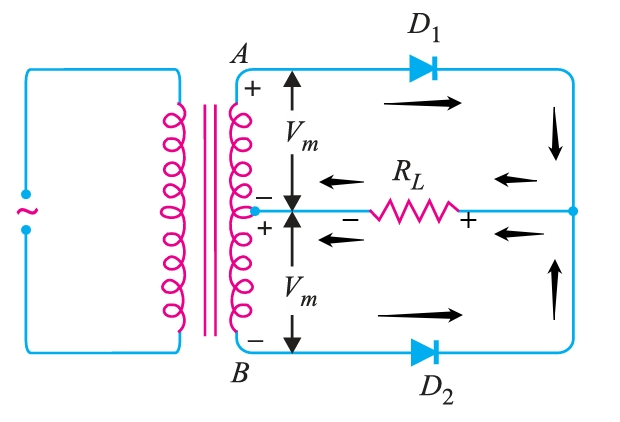
During the positive half-cycle of the secondary voltage, the end \(A\) of the secondary winding becomes positive, and end \(B\) becomes negative. This makes the diode \(D1\) forward-biased and the diode \(D2\) reverse-biased. Therefore, diode \(D1\) conducts while diode \(D2\) does not. The conventional current flow is through diode \(D1\), load resistor \(R_{L}\), and the upper half of the secondary winding, as shown by the dotted arrows. During the negative half-cycle, end \(A\) of the secondary winding becomes negative, while end \(B\) becomes positive. Therefore, diode \(D2\) conducts while diode \(D1\) does not. The conventional current flow is through diode \(D2\), load \(R_{L}\), and the lower half winding, as shown by solid arrows. The current in the load \(R_L\) is in the same direction for both half-cycles of input a.c. voltage. Therefore, d.c. is obtained across the load \(R_L\). Also, the polarities of the d.c. output across the load should be noted.
Suppose \(V_{m}\) is the maximum voltage across the half secondary winding. Fig. 16 shows the circuit at the instant secondary voltage reaches its maximum value in the positive direction. At this instant, diode \(D1\) is conducting while diode \(D2\) is non-conducting. Therefore, the entire secondary voltage appears across the non-conducting diode. Consequently, the peak inverse voltage is twice the maximum voltage across the half-secondary winding, i.e.
\[PIV = 2 V_{m}\]
Advantages
- Higher efficiency in the conversion of both halves of the AC input into DC output (Maximum efficiency is about \(81.2 ~%\))
- Produces smoother DC output because of lower ripple factor, \(\eta = 0.482\).
- The transformer’s secondary winding is used more effectively since both halves of the AC cycle contribute to rectification.
- A simpler design than a bridge rectifier because it requires only two diodes.
Disadvantages
- (i) It is difficult to locate the centre tap on the secondary winding.
- (ii) The d.c. output is small as each diode utilises only one-half of the transformer secondary voltage.
- (iii) The diodes used must have high peak inverse voltage.
Full-Wave Bridge Rectifier
The need for a centre-tapped power transformer is eliminated in the bridge rectifier. It contains four diodes, \(D1\), \(D2\), \(D3\), and \(D4\), connected to form a bridge, as shown in Fig. 17. The a.c. supply to be rectified is applied to the diagonally opposite ends of the bridge through the transformer. Between the two ends of the bridge, the load resistance \(R_{L}\) is connected.
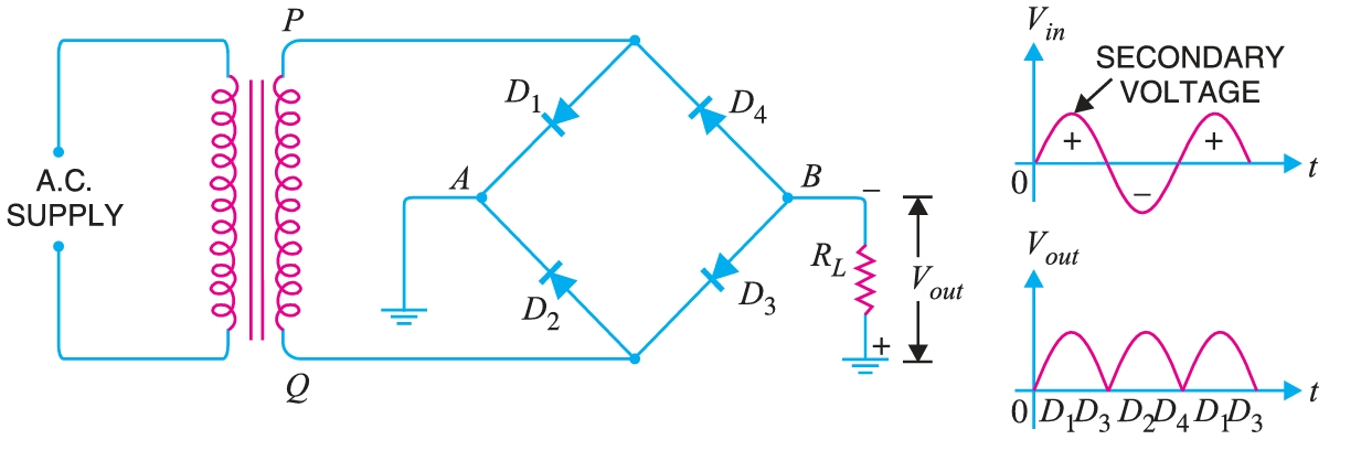
During the positive half-cycle of the secondary voltage, the end P of the secondary winding becomes positive, and end \(Q\) becomes negative. This makes diodes \(D1\) and \(D3\) forward-biased, while diodes \(D2\) and \(D4\) are reverse-biased. Therefore, only diodes \(D1\) and \(D3\) conduct. These two diodes will be in series through the load \(R_{L}\) as shown in Fig. 17. The conventional current flow is shown by dotted arrows. It may be seen that current flows from \(A\) to \(B\) through the load \(R_{L}\).
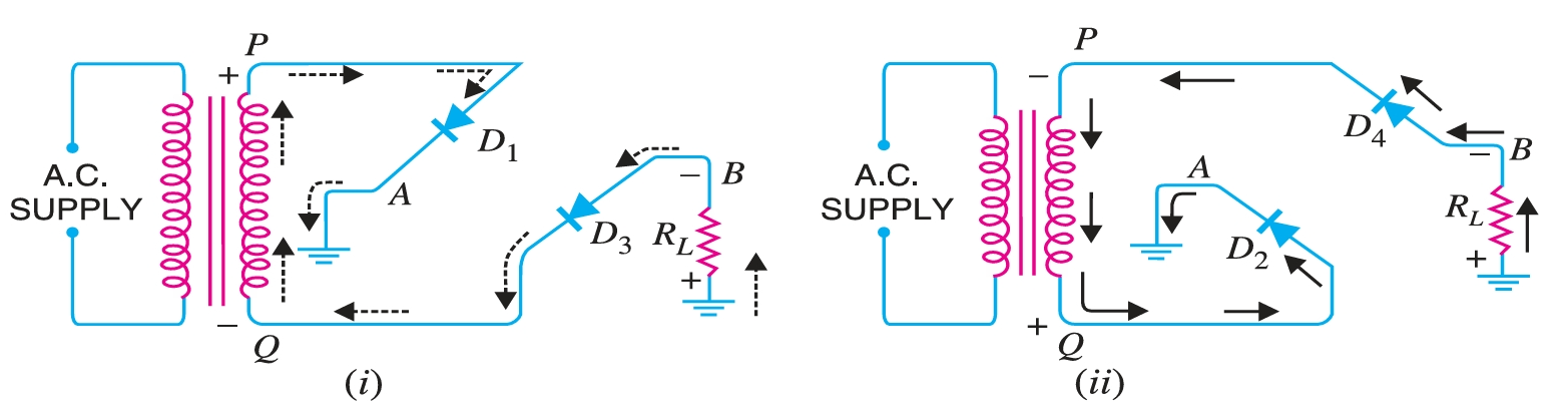
During the negative half-cycle of secondary voltage, end \(P\) becomes negative and end \(Q\) positive. This makes diodes \(D2\) and \(D4\) forward biased, whereas diodes \(D1\) and \(D3\) are reverse biased. Therefore, only diodes \(D2\) and \(D4\) conduct. These two diodes will be in series through the load \(R_{L}\) as shown in Fig. 18. The current flow is shown by the solid arrows. It may be seen that again current flows from \(A\) to \(B\) through the load, i.e., in the same direction as for the positive half-cycle. Therefore, d.c. output is obtained across load \(R_{L}\).
The peak inverse voltage (\(PIV\)) of each diode is equal to the maximum secondary voltage of the transformer. Suppose during the positive half cycle of the input a.c., end \(P\) of the secondary is positive and end \(Q\) negative. Under such conditions, diodes \(D1\) and \(D3\) are forward-biased while diodes \(D2\) and \(D4\) are reverse-biased. Since the diodes are considered ideal, diodes \(D1\) and \(D3\) can be replaced by wires.
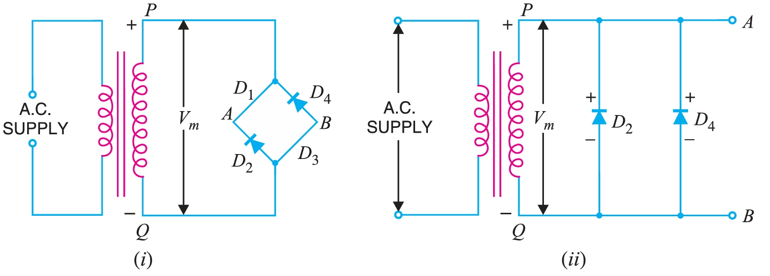
It is clear that two reverse-biased diodes (i.e., \(D2\) and \(D4\)) and the secondary of the transformer are in parallel. Hence \(PIV\) of each diode (\(D2\) and \(D4\)) is equal to the maximum voltage (\(V_{m}\)) across the secondary. Similarly, during the next half cycle, \(D2\) and \(D4\) are forward-biased, while \(D1\) and \(D3\) are reverse-biased. It is easy to see that reverse voltage across \(D1\) and \(D3\) is equal to \(V_{m}\). The output frequency of a full-wave rectifier is double the input frequency. A wave has a complete cycle when it repeats the same pattern. In Fig. 19, the input a.c. completes one cycle from 0° – 360°. However, the full-wave rectified wave completes 2 cycles in this period. Therefore, output frequency is twice the input frequency, i.e.
\[f_{out} = 2 f_{in}\]
Advantages
- (i) The need for a centre-tapped transformer is eliminated.
- (ii) The output is twice that of the centre-tap circuit for the same secondary voltage.
- (iii) The PIV is one-half that of the centre-tap circuit (for the same d.c. output).
Disadvantages
- (i) It requires four diodes.
- (ii) As during each half-cycle of a.c. input two diodes that conduct are in series; therefore, the voltage drop in the internal resistance of the rectifying unit will be twice as great as in the centre tap circuit. This is objectionable when the secondary voltage is small.
Efficiency of Full-Wave Rectifier
Let \(v = V_{m} \sin θ\) be the a.c. voltage to be rectified having a corresponding current, \(i = I_{m} \sin θ\). Let \(r_d\) and \(R_{L}\) be the diode resistance and load resistance, respectively. Obviously, the rectifier will conduct current through the load in the same direction for both half-cycles of input a.c. voltage. The instantaneous current \(i\) is given by :
- d.c. output power The output current is a pulsating direct current. Therefore, in order to find the d.c. power, the average current must be determined. \[I_{dc} = \frac{2I_{m}}{\pi}\] \[\therefore \text{d.c. power, } P_{dc} = I_{dc}^2 R_L = \left(\frac{2I_{m}}{\pi}\right)^2 R_L\]
- a.c. input power The current through the half wave rectifier circuit, \(I_{rms}\) is given as: \[I_{rms} = \sqrt{\frac{1}{2\pi} \int_0^{2\pi} i^2 ~d\theta}\] \[I_{rms} = \sqrt{\frac{1}{2\pi} \int_0^{2\pi} I_{m}^2 \sin^{2}\theta ~d\theta}\] \[I_{rms} = \sqrt{\frac{I_{m}^2}{2\pi} \int_0^{2\pi} \sin^{2}\theta ~d\theta}\] \[I_{rms} = \sqrt{\frac{I_{m}^2}{2\pi} \int_0^{2\pi} \sin^{2}\theta ~d\theta}\] \[I_{rms} = \sqrt{\frac{I_{m}^2}{2\pi} \int_0^{2\pi} \left[\frac{1 - \cos(2\theta)}{2}\right] ~d\theta}\] \[I_{rms} = \sqrt{\frac{I_{m}^2}{2\pi} \left[ \frac{\theta}{2} - \frac{1}{4}\sin(2\theta) \right]_0^{2\pi}}\] \[I_{rms} = \sqrt{\frac{I_{m}^2}{2\pi} \left[ \frac{2\pi}{2} - \frac{1}{4}\sin(4\pi) \right]}\] \[I_{rms} = \sqrt{\frac{I_{m}^2}{2\pi} [ \pi ]}\] \[I_{rms} = \sqrt{\frac{I_{m}^2}{2}}\] \[I_{rms} = \frac{I_{m}}{\sqrt{2}}\] The a.c. input power is given by: \[P_{ac} = I_{rms}^2 (r_d+R_L)\] For a full-wave rectified wave, we have, \[I_{rms}=\frac{I_m}{\sqrt{2}}\] \[\therefore \qquad P_{ac} = \left(\frac{I_m}{\sqrt{2}}\right)^2 (r_d+R_L)\]
- Full wave rectification efficiency \[\eta = \frac{P_{dc}}{P_{ac}} = \frac{\left(\frac{I_{m}}{\pi}\right)^2 R_L}{\left(\frac{I_m}{\sqrt{2}}\right)^2 (r_d+R_L)}\] \[\eta = \left(\frac{8}{\pi^2}\right)\times\frac{R_L}{(r_d+R_L)}\] \[\eta = 0.812\times\frac{R_L}{(r_d+R_L)} = \frac{0.812}{\left(\frac{R_L+r_d}{R_L}\right)} \] \[\eta = \frac{0.812}{\left(1+\frac{r_d}{R_L}\right)} \]
The efficiency will be maximum if \(r_d\) is negligible as compared to \(R_L\). \[\therefore \qquad \qquad \text{Maximum efficiency } = 81.2 ~\%\]
This is double the efficiency due to a half-wave rectifier. Therefore, a full-wave rectifier is twice as effective as a half-wave rectifier.
| S. No. | Particulars | Half-wave | Centre-tap | Bridge type |
|---|---|---|---|---|
| 1 | No. of diodes | \(1\) | \(2\) | \(4\) |
| 2 | Transformer necessary | no | yes | no |
| 3 | Max. efficiency | \(40.6 ~\%\) | \(81.2 ~\%\) | \(81.2 ~\%\) |
| 4 | Ripple factor | \(1.21\) | \(0.48\) | \(0.48\) |
| 5 | Output frequency | \(f_{in}\) | \(2f_{in}\) | \(2f_{in}\) |
| 6 | Peak inverse voltage | \(V_m\) | \(2V_m\) | \(V_m\) |
A comparison among the three rectifier circuits must be made with great care. Although the bridge circuit has some disadvantages, it is the best circuit from the viewpoint of overall performance. When the transformer cost is the main consideration in a rectifier assembly, we invariably use the bridge circuit. This is particularly true for large rectifiers, which have a low-voltage and a high-current rating.
Ripple Factor
A pulsating output of a rectifier contains a d.c. component and an a.c. component. The output of a rectifier consists of a d.c. component and an a.c. component (also known as ripple). The a.c. component is undesirable and accounts for the pulsations in the rectifier output. The effectiveness of a rectifier depends upon the magnitude of a.c. component in the output; the smaller this component, the more effective is the rectifier. The ratio of r.m.s. value of a.c. component to the d.c. component in the rectifier output is known as ripple factor i.e.
\[\text{Ripple factor} = \frac{\text{r.m.s. value of a.c component}}{\text{value of d.c. component}} = \frac{I_{ac}}{I_{dc}}\]
Therefore, ripple factor is very important in deciding the effectiveness of a rectifier. The smaller the ripple factor, the lesser the effective a.c. component and hence more effective is the rectifier.
The output current of a rectifier contains d.c. as well as a.c. component. The undesired a.c. component has a frequency of 100 Hz (i.e. double the supply frequency 50 Hz) is the ripple. It is a fluctuation superimposed on the d.c. component.
By definition, the effective (i.e. r.m.s.) value of total load current is given by : \[I_{rms} =\sqrt{I_{dc}^{2} + I_{ac}^{2}}\] or \[I_{ac} =\sqrt{I_{rms}^{2} - I_{dc}^{2}}\] Dividing throughout by \(I_{dc}\), we get,
\[\frac{I_{ac}}{I_{dc}} = \frac{\sqrt{I_{rms}^{2} - I_{dc}^{2}}}{I_{dc}}\]
But \(I_{ac}/I_{dc}\) is the ripple factor.
\[\therefore\qquad\qquad \text{Ripple factor} = \sqrt{\left(\frac{I_{rms}}{I_{dc}}\right)^{2} - 1}\]
For half-wave rectification
In half-wave rectification, \[I_{rms} = \frac{I_{m}}{2}\] \[I_{dc} = \frac{I_{m}}{\pi}\]
\[\therefore\qquad\qquad \text{Ripple factor} = \sqrt{\left(\frac{\frac{I_{m}}{2}}{\frac{I_{m}}{\pi}}\right)^2-1} = \sqrt{\left(\frac{\pi}{2}\right)^2-1} \]
\[\qquad\qquad \text{Ripple factor} = \sqrt{\left(\frac{\pi^2}{4}-1\right)}= 1.21 \]
It is clear that a.c. component exceeds the d.c. component in the output of a half-wave rectifier. This results in greater pulsations in the output. Therefore, half-wave rectifier is ineffective for conversion of a.c. into d.c.
For full-wave rectification.
In full-wave rectification, \[I_{rms} = \frac{I_{m}}{\sqrt{2}}\] \[I_{dc} = \frac{2I_{m}}{\pi}\]
\[\therefore\qquad\qquad \text{Ripple factor} = \sqrt{\left(\frac{\frac{I_{m}}{\sqrt{2}}}{\frac{2I_{m}}{\pi}}\right)^2-1} =\sqrt{\left(\frac{\pi}{2\sqrt{2}}\right)^2-1} \]
\[\therefore \qquad\qquad \text{Ripple factor} = \sqrt{\left(\frac{\pi^2}{8}\right)-1} =0.48 \]
i.e., \[\text{Ripple factor} = \frac{\text{effective a.c. component}}{\text{d.c. component}} = 0.48\]
This shows that in the output of a full-wave rectifier, the d.c. component is more than the a.c. component. Consequently, the pulsations in the output will be less than in half-wave rectifier. For this reason, full-wave rectification is invariably used for conversion of a.c. into d.c.
Filter Circuits
A rectifier is required to produce pure d.c. supply for use at various places in the electronic circuits. However, the output of a rectifier has pulsating character i.e., it contains a.c. and d.c. components. The a.c. component is undesirable and must be kept away from the load. If such a d.c. is applied in an electronic circuit, it will produce a hum.
A filter circuit is used to do so, removing (or filtering out) the a.c. component and allows only the d.c. component to reach the load.
A filter circuit is a device that removes the a.c. component of the rectifier output, but allows the d.c. component to reach the load.
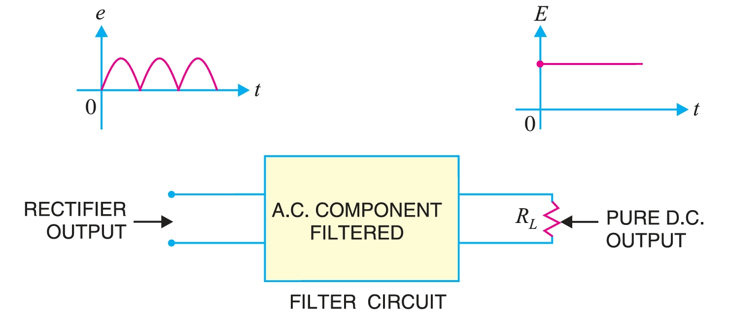
A filter circuit should be installed between the rectifier and the load, as shown in Fig. 1. A filter circuit is generally a combination of inductors (\(L\)) and capacitors (\(C\)). The filtering action of \(L\) and \(C\) depends upon the basic electrical principles. A capacitor passes a.c. readily, but does not pass d.c. at all. A capacitor offers infinite reactance to d.c.
For d.c., \(f = 0\).
\[X_C = \frac{1}{2\pi fC} = \frac{1}{2\pi\times 0 \times C} = \infty\]
Hence, a capacitor does not allow d.c. to pass through it.
On the other hand, an inductor opposes a.c. but allows d.c. to pass through it. The inductive reactance is given as:
\[X_L = 2\pi fL \]
For d.c., \(f = 0\) and, therefore, \(X_L = 0\). Hence inductor passes d.c. quite readily. For a.c., it offers opposition and drops a part of it.
It then becomes clear that a suitable network of \(L\) and \(C\) can effectively remove the a.c. component, allowing the d.c. component to reach the load.
Types of Filter Circuits
The most commonly used filter circuits are the capacitor filter, the choke input filter, the capacitor input filter (\(\pi\)-filter), and the \(\pi\)-filter. We shall discuss these filters in turn.
Capacitor filter.
Fig. 2 shows a typical capacitor filter circuit. It consists of a capacitor \(C\) placed in parallel with the load \(R_L\) across the rectifier output. The pulsating direct voltage of the rectifier is applied across the capacitor. As the rectifier voltage increases, it charges the capacitor and also supplies current to the load.
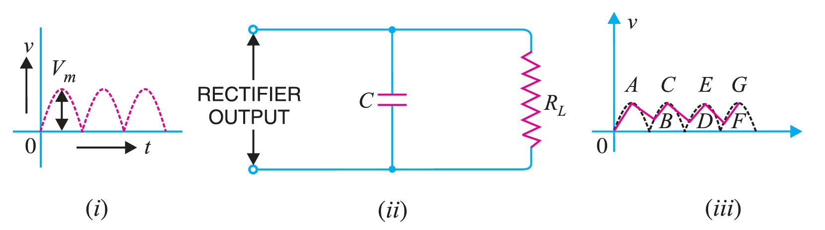
At the end of the quarter cycle [Point A in Fig. 2], the decrease. As this occurs, the capacitor discharges through the load, and the voltage across it (i.e., across a parallel combination of \(R-C\)) decreases as shown by the line \(AB\) in Fig 2. The voltage across the load will decrease only slightly, because the next voltage peak immediately follows and recharges the capacitor. This process is repeated, and the output voltage waveform becomes \(ABCDEFG\). It may be seen that very little ripple is left in the output. Moreover, the output voltage is higher as it remains substantially near the peak value of the rectifier output voltage. The capacitor filter circuit is extremely popular due to its low cost, small size, low weight, and good performance. For small load currents, this type of filter is preferred. It is commonly used in transistor radio battery eliminators.
Choke input filter
Fig. 3 shows a typical choke input filter circuit. It consists of a choke \(L\) connected in series with the rectifier output and a filter capacitor \(C\) across the load. Only a single filter section is shown, but several identical sections are often used to reduce the pulsations as effectively as possible. The pulsating output of the rectifier is applied across terminals \(1\) and \(2\) of the filter circuit.
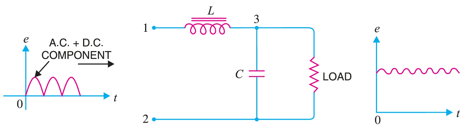
The pulsating output of the rectifier contains a.c. and d.c. components. The choke offers high opposition to the passage of a.c. component but negligible opposition to the d.c. component. The result is that most of the a.c. component appears across the choke while the whole of the d.c. The component passes through the choke on its way to the load. This results in the reduced pulsations at terminal \(3\)
At terminal \(3\), the rectifier output contains d.c. component and the remaining part of the a.c. A component that has managed to pass through the choke. Now, the low reactance of the filter capacitor bypasses the a.c. component but prevents the d.c. component to flow through it. Therefore, only d.c. component reaches the load. In this way, the filter circuit has removed the a.c. component. component from the rectifier output, allowing d.c. component to reach the load.
Capacitor input filter
Fig. 4 shows a typical capacitor-input filter, or \(\pi-\)filter. It consists of a filter capacitor \(C_1\) connected across the rectifier output, a choke \(L\) in series, and another filter capacitor \(C_2\) connected across the load.
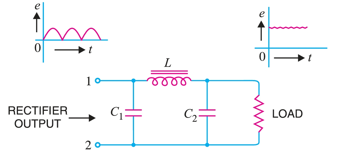
Only one filter section is shown, but several identical sections are often used to enhance smoothing. The pulsating output from the rectifier is applied across the input terminals (i.e., terminals \(1\) and \(2\)) of the filter. The filtering action of the three components, viz, \(C_1\), \(L\), and \(C_2\) of this filter, is described below :
- (a) The filter capacitor \(C_1\) offers low reactance to a.c. component of the rectifier output, while it offers infinite reactance to the d.c. component. Therefore, capacitor \(C_1\) bypasses an appreciable amount of a.c. component while the d.c. component continues its journey to the choke \(L\).
- (b) The choke \(L\) offers high reactance to the a.c. component, but it offers almost zero reactance to the d.c. component. Therefore, it allows the d.c. component to flow through it, while the *unbypassed a.c. component is blocked.
- (c) The filter capacitor \(C_2\) bypasses the a.c. The component that the choke has failed to block. Therefore, only d.c. component appears across the load, and that is what we desire.
Zener Diode
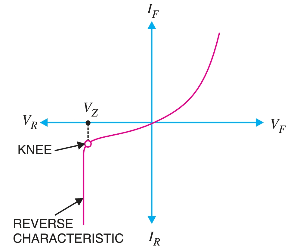
A zener diode is a special type of diode that is designed to operate in the reverse breakdown region. An ordinary diode operated in this region will usually be destroyed due to excessive current. This is not the case for the zener diode. A zener diode is heavily doped to reduce the reverse breakdown voltage. This causes a very thin depletion layer. As a result, a zener diode has a sharp reverse breakdown voltage \(V_{Z}\). This is clear from the reverse characteristic of zener diode.
The reverse characteristic drops in an almost vertical manner at reverse voltage \(V_{Z}\). As the curve reveals, two things happen when \(V_{Z}\) is reached :
- (i) The diode current increases rapidly.
- (ii) The reverse voltage \(V_{Z}\) across the diode remains almost constant.
In other words, the zener diode operated in this region will have a relatively constant voltage across it, regardless of the value of current through the device. This permits the zener diode to be used as a voltage regulator.
When the reverse bias on a \(p-n\) diode is increased, a critical voltage, called the breakdown voltage, is reached, where the reverse current increases sharply to a high value. The breakdown region is the knee of the reverse characteristic, as shown in Fig. 1.
The satisfactory explanation of this breakdown of the junction was first given by the American scientist C. Zener. Therefore, the breakdown voltage is sometimes called zener voltage and the sudden increase in current is known as zener current. The breakdown or zener voltage depends upon the amount of doping. If the diode is heavily doped, the depletion layer will be thin, and the breakdown of the junction will occur at a lower reverse voltage; such a diode is known as a zener diode. On the other hand, a lightly doped diode has a higher breakdown voltage.
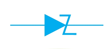
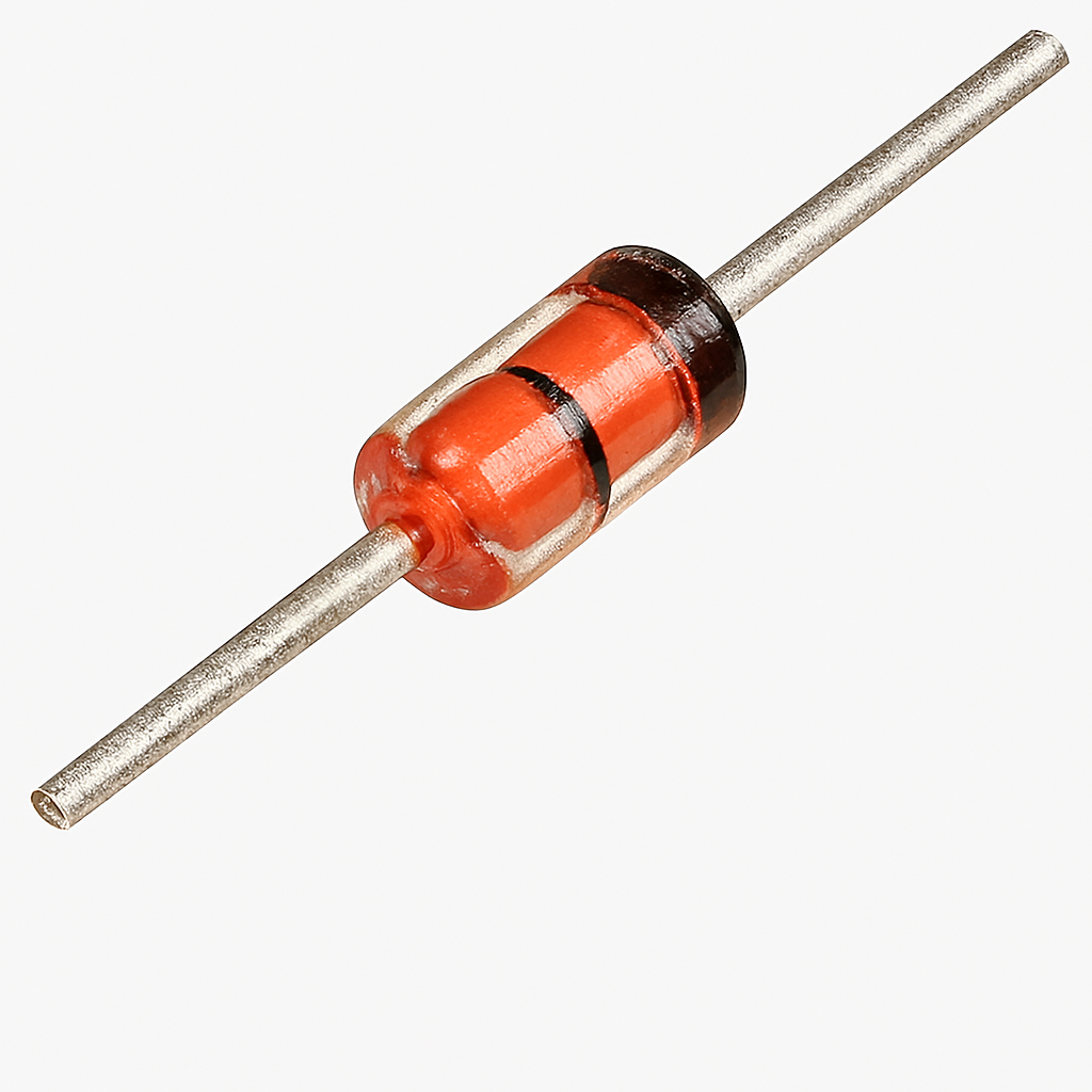
A properly doped crystal diode that has a sharp breakdown voltage is known as a zener diode. Fig. 2 shows the symbol of a zener diode. It appears to be just like an ordinary diode, except that the bar is bent into a Z-shape. The following points may be noted about the Zener diode:
- (i) A zener diode is like an ordinary diode except that it is properly doped so as to have a sharp breakdown voltage.
- (ii) A zener diode is always reverse connected, i.e., it is always reverse-biased.
- (iii) A zener diode has a sharp breakdown voltage, called zener voltage, \(V_Z\).
- (iv) When forward-biased, its characteristics are just those of an ordinary diode.
- (v) The zener diode is not immediately burnt just because it has entered the breakdown region. As long as the external circuit connected to the diode limits the diode current to less than the burnout value, the diode will not burn out.
Zener Diode as Voltage Stabiliser
A zener diode can be used as a voltage regulator to provide a constant voltage from a source whose voltage may vary over a sufficient range. The circuit arrangement is shown in Fig. 3. The zener diode with zener voltage \(V_Z\) is reverse-biased across the load \(R_L\), across which a constant output is desired. The series resistance \(R\) absorbs the output voltage fluctuations, maintaining a constant voltage across the load. It may be noted that the zener will maintain a constant voltage \(V_Z (= E_0)\) across the load so long as the input voltage does not fall below \(V_Z\).
When the circuit is properly designed, the load voltage \(E_0\) remains essentially constant (equal to \(V_Z\)) even as the input voltage \(E_i\) and load resistance \(R_L\) vary widely.
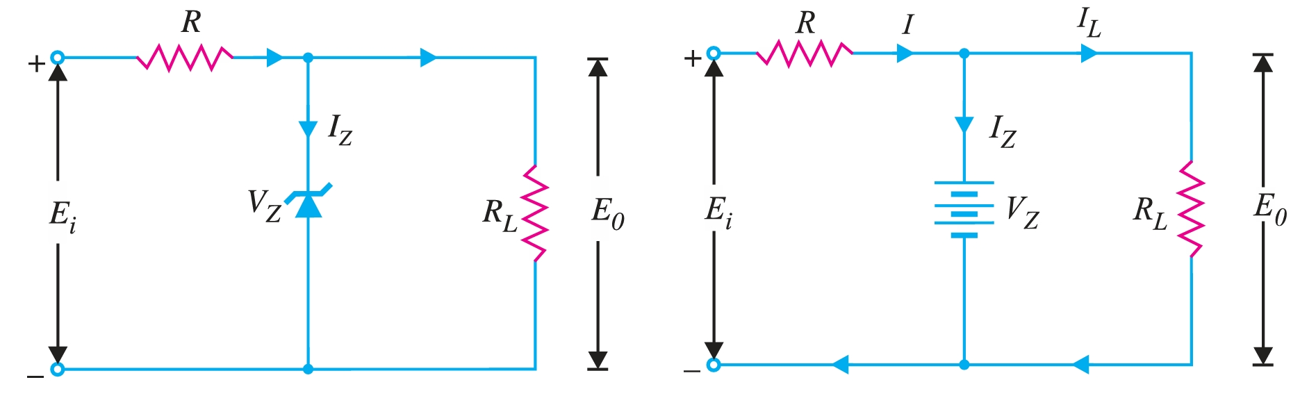
- (i) Suppose the input voltage increases. Since the zener is in the breakdown region, the zener diode is equivalent to a battery with voltage \(V_Z\), as shown in Fig. 3. It is clear that the output voltage remains constant at \(V_Z (= E_0)\). The excess voltage is dropped across the series resistance R, which increases the total current \(I\). The zener will conduct the increase of current \(I\) while the load current remains constant. Hence, output voltage \(E_0\) remains constant irrespective of the changes in the input voltage \(E_i\).
- (ii) Now suppose that the input voltage is constant, but the load resistance \(R_L\) decreases. This will increase the load current. The extra current cannot come from the source because a drop in \(R\) (and hence source current \(I\)) will not change as the zener is within its regulating range. The additional load current will come from a decrease in zener current \(I_Z\). Consequently, the output voltage remains constant.
\[\text{Voltage drop across R, } V_R = E_i − E_0\] \[\text{Current through R, } I = I_Z + I_L\] Applying Ohm’s law, such that, \(V_R = IR\), we have,
\[R = \frac{E_i − E_0}{I_Z + I_L}\]
The analysis of Zener diode circuits is quite similar to that applied to the analysis of semiconductor diodes. The first step is to determine the state of the zener diode, i.e., whether the zener is in the ON state or OFF state. Next, the zener is replaced by its appropriate model. Finally, the unknown quantities are determined from the resulting circuit.
Fixed Input Voltage and Load Resistance
This is the simplest case, shown in Fig. 4. Here, the applied voltage \(E_i\) and the load \(R_L\) are fixed. The first step is to find the state of the Zener diode. This can be determined by removing the zener from the circuit and calculating the voltage \(V\) across the resulting open circuit.
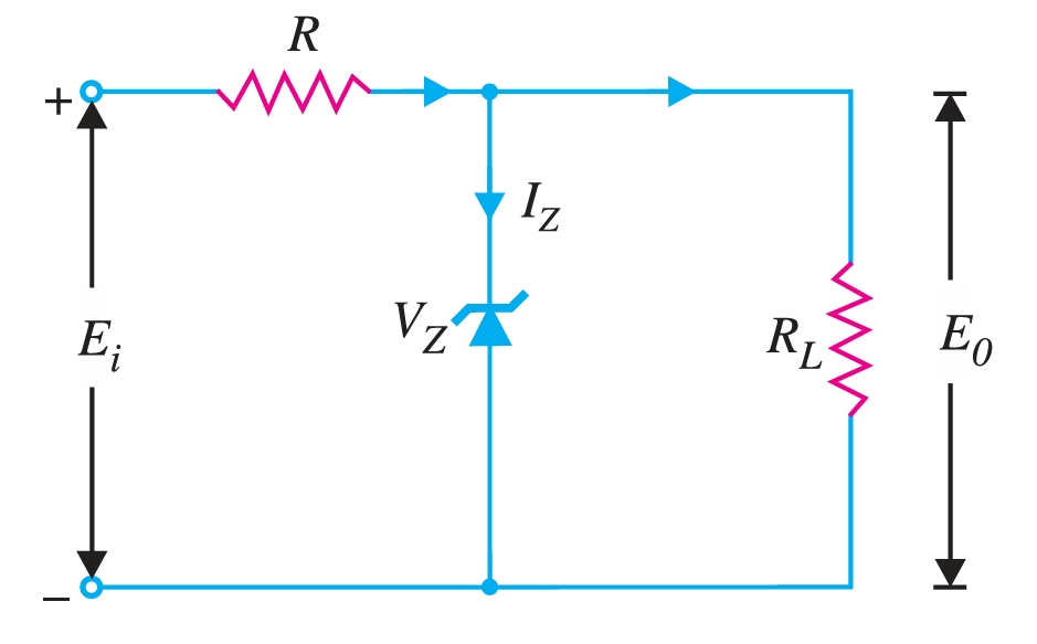
\[V = E_0 = \frac{R_L E_i}{R + R_L}\]
If \(V \geq V_Z\), the zener diode is in the ON state and its equivalent model can be substituted as shown in Fig. 2. If \(V < V_Z\), the diode is in the OFF state.
- (i) On state \[E_0 = V_Z \] \[I_Z = I - I_L \quad\text{where,}\quad I_L = \frac{E_0}{R_L} \quad\text{and}\quad I = \frac{E_i-E_0}{R}\] \[\text{Power dissipated in Zener, } P_Z = V_Z I_Z\]
- (ii) Off state \[I = I_L \text{ and } I_Z = 0\] \[V_R = E_i − E_0 \quad\text{and}\quad V = E_0 \quad (V < V_Z)\] \[\therefore P_Z = V I_Z = V \times 0 = 0\]
Fixed Input Voltage and Variable Load resistance.
This case is shown in Fig. 4. Here, the applied voltage (\(E_i\)) is fixed while the load resistance \(R_L\) (and hence the load current \(I_L\)) changes. Note that there is a definite range of \(R_L\) values (and hence \(I_L\) values) which will ensure the zener diode to be in ON state. Let us calculate that range of values.
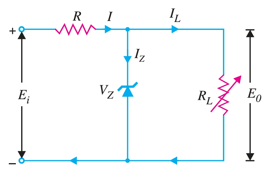
- (i) \(R_{L\text{min}}\) and \(I_{L\text{max}}\)
Once the zener is in the ON state, load voltage \(E_0 (= V_Z)\) is constant. As a result, when load resistance is minimum (i.e., \(R_{L\text{min}}\)), load current will be maximum (\(I_L = E_0/R_L\)). In order to find the minimum load resistance that will turn the zener on, we simply calculate the value of \(R_L\) that will result in \(E_0 = V_Z\), i.e., \[E_0 = V_Z = \frac{R_L E_i}{R + R_L}\] \[ V_Z (R + R_L) = R_L E_i\] \[ V_Z R + V_Z R_L = R_L E_i\] \[ V_Z R = R_L E_i - V_Z R_L\] \[ V_Z R = R_L (E_i - V_Z)\] \[R_L = \frac{V_Z R}{E_i - V_Z}\] Hence, \(R_{L\text{min}}\) is obtained as: \[\therefore\quad R_{L\text{min}} = \frac{R V_Z}{E_i - V_Z}\] This is the minimum load resistance required to ensure the zener is in the ON state. Any load resistance below this value will result in a voltage \(E_{0}\) across the load less than \(V_{Z}\), and the zener will be in the OFF state. \[\text {Clearly;}\qquad\qquad I_{L\text{max}} = \frac{E_0}{R_{L\text{min}}} = \frac{V_Z}{R_{L\text{min}}}\] - (ii) \(I_{L\text{min}}\) and \(R_{L\text{max}}\) It is easy to see that when the load resistance is maximum, the load current is \(L_{min}\). Now, \[\text{Zener current, } I_Z = I − I_L\] When the zener is in the ON state, \(I\) remains fixed. That is, the Voltage across \(R\), \(V_R = E_i − E_0\) and \(I = V_R/R\). As \(E_i\) and \(E_0\) are fixed, \(I\) remains the same. This means that when \(I_L\) is maximum, \(I_Z\) will be minimum. On the other hand, when \(I_L\) is minimum, \(I_Z\) is maximum. If the maximum current that a zener can carry safely is \(I_{ZM}\), then \[I_L = I - I_{ZM}\] \[R_{L\text{max}} = \frac{E_0}{I_{L\text{min}}} = \frac{V_Z}{I_{L\text{min}}}\] If the load resistance exceeds this limiting value, the current through the zener will exceed \(I_{ZM}\) and the device may burn out.
Fixed load resistance and Variable input voltage.
This case is shown in Fig. 5. Here, the load resistance \(R_L\) is fixed while the applied voltage (\(E_i\)) changes. Note that there is a definite range of \(E_i\) values that will ensure that the zener diode is in the ON state. Let us calculate that range of values.
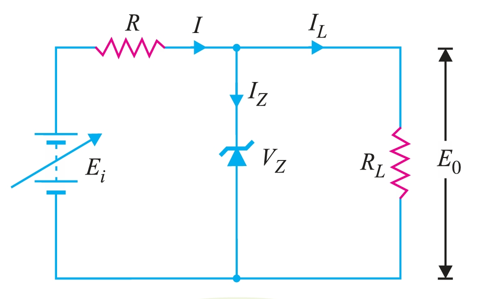
- (i) \(E_{i(\text{min})}\).
To determine the minimum applied voltage that will turn the zener on, simply calculate the value of \(E_i\) that will result in the load voltage, \(E_0 = V_Z\), i.e., \[E_0 = V_Z = \frac{R_L E_i}{R + R_L}\] \[\therefore \quad E_{i(\text{min})} = \frac{(R + R_L)V_Z}{R_L}\] - (ii) \(E_{i(\text{max})}\) Now, \[\text{current through } R, I = I_Z + I_L\] Since \(I_L (= E_0/R_L = V_Z/R_L)\) is fixed, the value of \(I\) will be maximum when zener current is maximum, i.e., \[I_{\text{max}} = I_{ZM} + I_L\] Now \[E_i= I R + E_0\] Since \(E_0 (= V_Z)\) is constant, the input voltage will be maximum when \(I\) is maximum. \[\therefore \quad E_{i(\text{max})} = I_{\text{max}} R + V_Z\] which means, \[\therefore \quad E_{i(\text{max})} = (I_{ZM} + I_L) R + V_Z\] \[\therefore \quad E_{i(\text{max})} = \left(I_{ZM} + \frac{V_Z}{R_L}\right) R + V_Z\]
Light-Emitting Diode (LED)
A light-emitting diode (LED) is a diode that gives off visible light when forward biased.
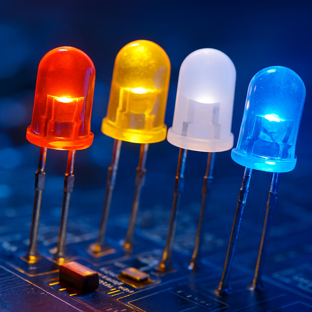
Light-emitting diodes are not made from silicon or germanium but are made by using elements like gallium, phosphorus and arsenic. By varying the quantities of these elements, it is possible to produce light of different wavelengths with colours that in clude red, green, yellow and blue. For example, when a LED is manufactured using gallium arsenide, it will produce a red light. If the LED is made with gallium phosphide, it will produce a green light.
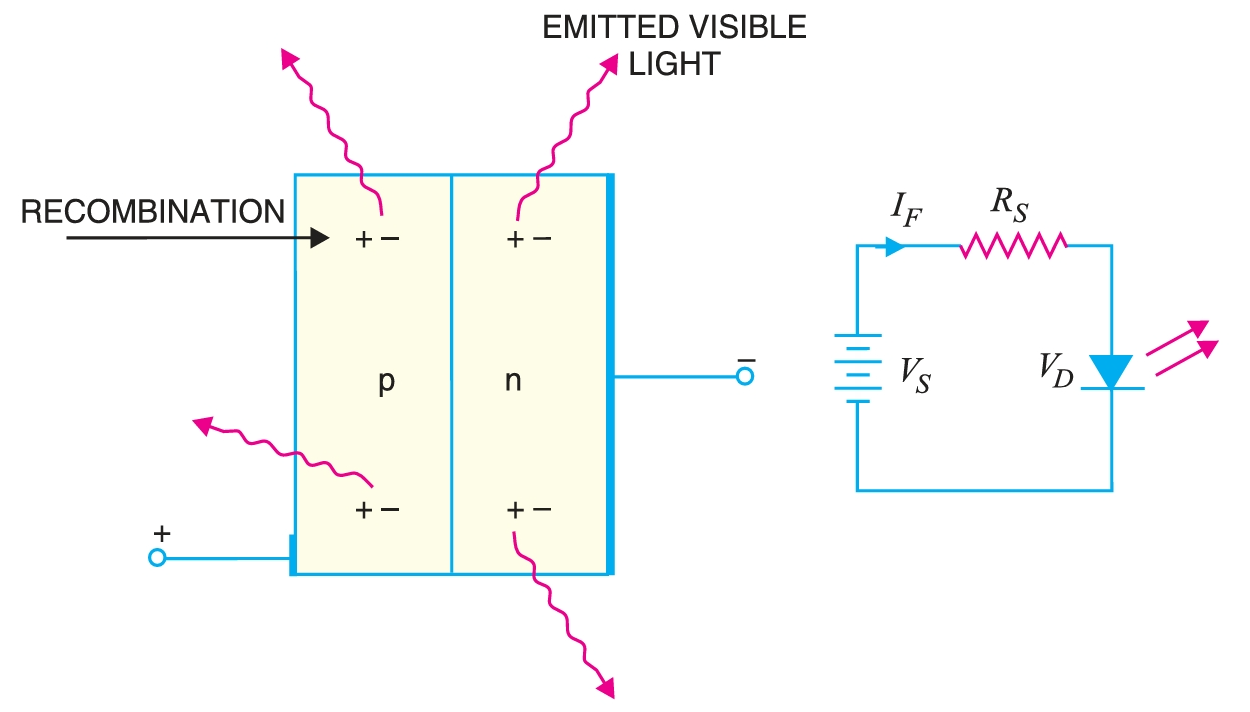
When light-emitting diode (LED) is forward biased as shown in Fig. 2, the electrons from the \(n\)-type material cross the \(pn\) junction and recombine with holes in the \(p\)-type material. These free electrons are in the conduction band and at a higher energy level than the holes in the valence band. When recombination takes place, the recombining electrons release energy in the form of heat and light.
In germanium and silicon diodes, almost the entire energy is given up in the form of heat and emitted light is insignificant. However, in materials like gallium arsenide, the number of photons of light energy is sufficient to produce quite intense visible light.
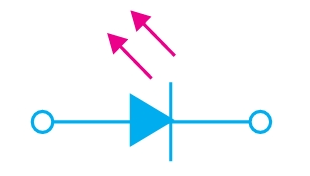
Fig. 3 shows the schematic symbol for a LED. The arrows are shown as pointing away from the diode, indicating that light is being emitted by the device when forward biased. The forward voltage ratings of most LEDs is from \(1~V\) to \(3~V\) and forward current ratings range from 20 \(mA\) to 100 \(mA\). In order that current through the LED does not exceed the safe value, a resistor \(R_S\) is connected in series with it as shown in Fig. 2. The input voltage is \(V_S\) and the voltage across LED is \(V_D\)
\[\therefore \hspace{1cm}R_S = V_S - V_D\] \[\therefore \hspace{1cm}I_F = \frac{V_S - V_D}{R_S}\]
Multicolour LEDs
A LED that emits one colour when forward biased and another colour when reverse biased is called a multicolour LED. It actually contain two \(pn\) junctions that are connected in reverse-parallel i.e., they are in parallel with anode of one being connected to the cathode of the other. If positive potential is applied to the top terminal as shown in Fig. 4, the \(pn\) junction on the left will light. The device current passes through the left pn junction. If the polarity of the voltage source is reversed, the pn junction on the right will light. The direction of device current has reversed and is now passing through the right pn junction.
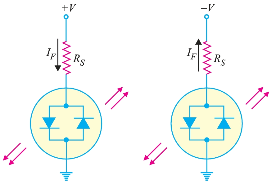
Multicolour LEDs are typically red when biased in one direction and green when biased in the other. If a multicolour LED is switched fast enough between two polarities, the LED will produce a third colour. A red/green LED will produce a yellow light when rapidly switched back and forth between biasing polarities.
Advantages of LED
The light-emitting diode (LED) is a solid-state light source. LEDs have replaced incandescent lamps in many applications because they have the following advantages :
- (i) Low voltage
- (ii) Longer life (more than 20 years)
- (iii) Fast on-off switching
Applications of LEDs
The LED is a low-power device. The power rating of a LED is of the order of milliwatts. This means that it is useful as an indicator but not good for illumination. Probably the two most common applications for visible LEDs are (i) as a power indicator (ii) seven-segment display (iii) Indoor and Outdoor Lighting and (iv) LED displays.
Power indicator.
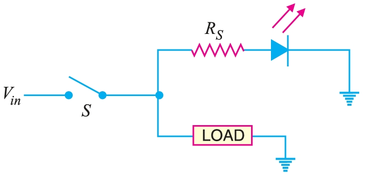
A LED can be used to indicate whether the power is on or not. Fig. 5 shows the simple use of the LED as a power indicator. When the switch \(S\) is closed, power is applied to the load. At the same time current also flows through the LED which lights, indicating power is on. The resistor \(R_S\) in series with the LED Fig. 5 ensures that current rating of the LED is not exceeded.
Seven-segment display
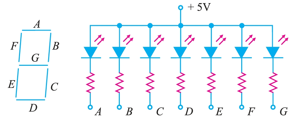
LEDs are often grouped to form seven-segment display. Fig. 6 shows the front of a seven segment display. It contains seven LEDs (\(A\), \(B\), \(C\), \(D\), \(E\), \(F\) and \(G\)) shaped in a figure of \(8\). Each LED is called a segment. If a particular LED is forward biased, that LED or segment will light and produces a bar of light. By forward biasing various combinations of seven LEDs, it is possible to display any number from 0 to 9. For example, if LEDs \(A\), \(B\), \(C\), \(D\) and \(G\) are lit (by forward biasing them), the display will show the number \(3\). Similarly, if LEDs \(C\), \(D\), \(E\), \(F\), \(A\) and \(G\) are lit, the display will show the number \(6\). To get the number \(0\), all segments except \(G\) are lit. External series resistors are included to limit currents to safe levels. The anodes of all seven LEDs are connected to a common positive voltage source of +5 V. This arrangement is known as common-anode type. In order to light a particular LED, the particular is grounded to complete the forward-biased circuit for the LED which makes it lit.
Indoor and Outdoor Lighting
White light-emitting diodes (LEDs) have become the dominant technology in modern lighting due to their efficiency, longevity, and versatility. Commercially available white LEDs are produced using several approaches, each with distinct advantages.
The most common type is the phosphor-converted LED (pc-LED). In this design, a blue LED chip (typically based on GaN/InGaN) is coated with a yellow-emitting phosphor such as cerium-doped yttrium aluminum garnet (\(YAG:Ce^{3+}\)). The mixture of blue and yellow light appears white to the human eye. These LEDs are inexpensive, efficient, and widely used in general illumination, though they often have limited color rendering because of weak red emission.

Another approach is the multi-chip RGB LED, which combines separate red, green, and blue LEDs in one package. By adjusting the relative intensities, manufacturers can produce pure white light or tune the color temperature. RGB LEDs offer excellent color rendering and flexibility, but they are more complex to drive and can suffer from color imbalance over time.
LED Display
Recent developments include hybrid LEDs that use blue chips with multiple phosphors (green and red) or advanced materials like quantum dots and perovskites. These provide improved spectral balance, higher color rendering index (CRI), and tunable correlated color temperature (CCT). Such LEDs are increasingly used in displays, medical lighting, and applications requiring precise color fidelity.
An LED display is a flat panel display technology that uses light-emitting diodes (LEDs) as pixels to produce images. Each pixel is formed by one or more LEDs, which emit light directly when an electric current passes through them. Unlike LCDs, which require a backlight, LED displays are self-emissive, meaning they generate their own light. This property gives them high brightness, excellent contrast, and wide viewing angles.

LED displays are broadly classified into direct-view LED displays and LED-backlit LCDs. Direct-view LED displays are commonly used in large outdoor billboards, stadium screens, and indoor video walls. They consist of arrays of red, green, and blue LEDs that combine to produce full-color images. The pixel pitch (distance between LEDs) determines resolution; smaller pitches allow higher-definition images suitable for close viewing.
LED-backlit LCDs, on the other hand, use LEDs as a backlight source for liquid crystal panels. This improves energy efficiency, color quality, and thinness compared to older CCFL backlights.
The key advantages of LED displays includes, high brightness suitable for outdoor use, energy efficiency compared to traditional display technologies, long lifespan and durability and finally the flexibility in size and shape, enabling curved or modular video walls.
Applications range from advertising billboards, traffic signs, and stadium scoreboards to indoor video walls, televisions, smartphones, and laptops. With advances in micro-LED and OLED technologies, LED displays continue to evolve, offering higher resolution, better color rendering, and thinner, more flexible designs.
Photo diode
A Photo diode is a reverse-biased silicon or germanium \(pn\) junction in which reverse current in creases when the junction is exposed to light. The reverse current in a photo diode is directly proportional to the intensity of light falling on its \(pn\) junction. This means that greater the intensity of light falling on the \(pn\) junction of photo diode, the greater will be the reverse current.
When a rectifier diode is reverse biased, it has a very small reverse leakage current. The same is true for a photo diode. The reverse current is produced by thermally generated electron hole pairs which are swept across the junction by the electric field created by the reverse voltage. In a rectifier diode, the reverse current increases with temperature due to an increase in the number of electron-hole pairs. A photo diode differs from a rectifier diode in that when its \(pn\) junction is exposed to light, the reverse current increases with the increase in light intensity and vice-versa.
This is explained as follows. When light (photons) falls on the \(pn\) junction, the energy is imparted by the photons to the atoms in the junction. This will create more free electrons (and more holes). This is true only if the light energy is applied at the junction. If it is applied to the crystal at some distance from the junction, the free electrons and holes will recombine (thus neutralising each other) before they can join the flow of reverse current. These additional free electrons will increase the reverse current.
As the intensity of light incident on the \(pn\)junction increases, the reverse current also increases. In other words, as the incident light intensity increases, the resistance of the device (photo diode) decreases. It is for this reason that semiconductor devices such as diodes and transistors are usually enclosed in opaque case to protect them from light. Those diodes or transistors which are used for light-detecting, on the other hand, must be encased in transparent plastic or glass so that light may fall on them.
Photo diode package.
Fig. 1 shows a typical photo diode package. It consists of a \(pn\) junction mounted on an insulated substrate and sealed inside a metal case. A glass window is mounted on top of the case to allow light to enter and strike the \(pn\) junction. The two leads extending from the case are labelled anode and cathode. The cathode is typically identified by a tab extending from the side of the case.
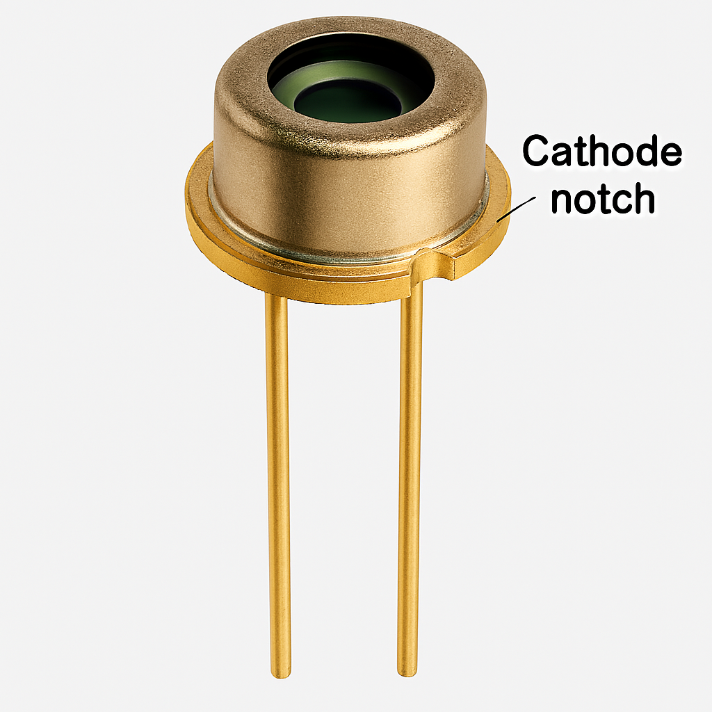
Fig. 2 shows the basic photo diode circuit. The circuit has reverse biased photo diode, resistor \(R\) and d.c. supply.
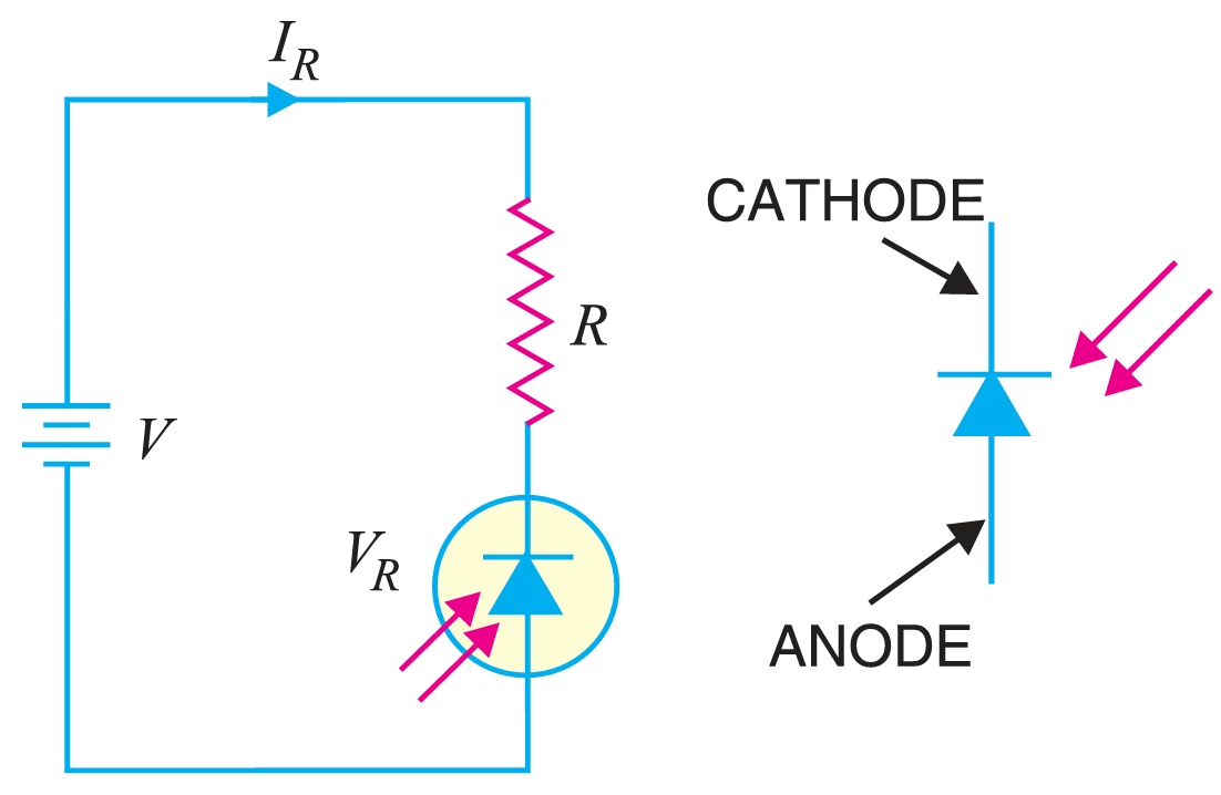
The operation of the photo diode is as under :
- (i) When no light is incident on the \(pn\) junction of photo diode, the reverse current \(I_R\) is extremely small. This is called dark current. The resistance of photo diode with no incident light is called dark resistance (R_R). Hence, the Dark resistance of photo diode is expressed as, \[R_R = \frac{V_R}{\text{Dark Current}}\]
- (ii) When light is incident on the \(pn\) junction of the photo diode, there is a transfer of energy from the incident light (photons) to the atoms in the junction. This will create more free electrons (and more holes). These additional free electrons will increase the reverse current.
- (iii) As the intensity of light increases, the reverse current \(I_R\) goes on increasing till it becomes maximum. This is called saturation current.
Characteristics of Photo diode
There are two important characteristics of photo diode.
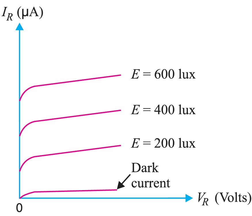
- (i) Reverse voltage-Reverse current curve. Fig. 3 shows the graph between reverse current (\(I_R\)) and reverse voltage (\(V_R\)) for various illumination levels. The reverse current \(I_R\) increases as the illumination (\(E\)) on the \(pn\) junction of photo diode is increased for a given reverse-biased voltage \(V_R\).
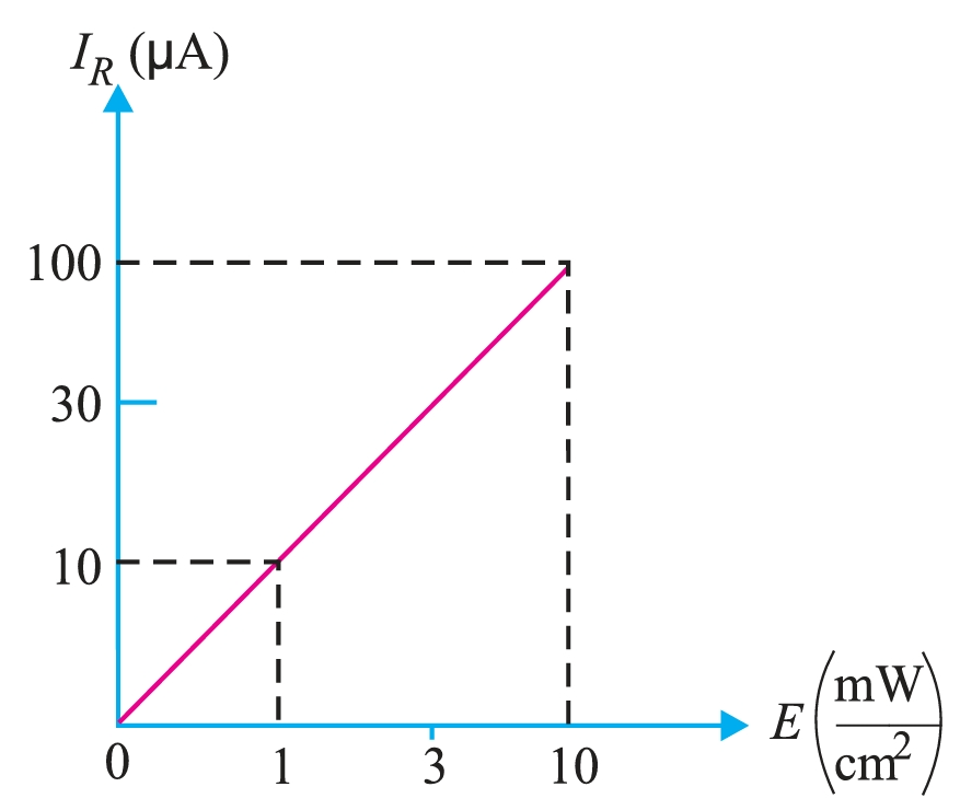
- (ii) Reverse current-Illumination curve. Fig. 4 shows the graph between reverse current (\(I_R\)) and illumination (\(E\)) of a photo diode. The reverse current is shown on the vertical axis and is measured in \(\mu A\). The illumination is indicated on the horizontal axis and is measured in \(mW/cm^{2}\). Note that graph is a straight line passing through the origin. \[\therefore I_R = m~E\]
where, \(m\) = slope of the straight line. The quantity \(m\) is called the sensitivity of the photo diode.
Applications of Photo diodes
There are a large number of applications of photo diodes. However, we shall give two applications of photo diodes by way of illustration.
Alarm circuit using Photo diode.
Light from a light source is allowed to fall on a photo diode fitted in the doorway. The reverse current \(I_R\) will continue to flow so long as the light beam is not broken. If a person passes through the door, light beam is broken and the reverse current drops to the dark current level. As a result, an alarm is sounded.
Counter circuit using photo diode
A photo diode may be used to count items on a conveyor belt. A source of light sends a concentrated beam of light across a conveyor to a photo diode. As the object passes, the light beam is broken, \(I_R\) drops to the dark current level and the count is increased by one.