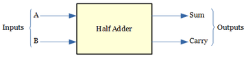
Half Adder:
In the realm of digital electronics, the concept of arithmetic and logic operations is foundational to building complex digital systems. Among these operations, addition holds a significant place. In order to perform addition on binary numbers, we utilize components called adders. A fundamental building block in this context is the "Half Adder." This article delves into the intricacies of the Half Adder, its operations, and its implementation using NAND gates.
Introduction:
A Half Adder is a combinatorial digital circuit that is used to add two single-bit binary numbers together. The term "half" indicates its limitation to dealing with only two input bits, thereby rendering it unsuitable for carrying over any previous carry generated from prior additions. The primary goal of a Half Adder is to calculate the sum and carry bits for the two input bits.
Basic Operations:
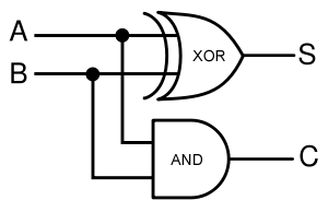
A Half Adder performs two essential operations: sum and carry generation. Let's consider two input bits: A and B. The corresponding operations are as follows:
Sum (\(S\)) Bit Calculation: The sum bit (\(S\)) is the result of the binary addition of the input bits A and B. It signifies the least significant bit (LSB) of the addition operation.
Mathematically, \(S\) = A XOR B (XOR denotes the exclusive OR operation)
Carry (C) Bit Generation: The carry bit (C) indicates whether there's a carry generated during the addition of the input bits. It signifies the most significant bit (MSB) of the addition operation.
Mathematically, C = A AND B (AND denotes the logical AND operation)
NAND Implementation of Half Adder:
Half Adder can be constructed using NAND gates. A NAND gate is a universal gate, which means that it can be used to implement all other basic logic gates like AND, OR, and NOT. Therefore, using NAND gates for the implementation of a Half Adder provides a versatile and efficient solution. A NAND gate produces an output that is the inverse of the result from an AND gate. Its output is LOW (0) only when both inputs are HIGH (1). Otherwise, the output is HIGH (1). Symbolically, the behavior of a NAND gate is represented as:
| A | B | Output |
|---|---|---|
| 0 | 0 | 1 |
| 0 | 1 | 1 |
| 1 | 0 | 1 |
| 1 | 1 | 0 |
The implementation of a Half Adder using NAND gates involves the use of these gates to recreate the XOR and AND operations that define the sum and carry calculations, respectively.
Sum (\(S\)) Bit Calculation: To implement the XOR operation using NAND gates, the inputs are first NANDed together and then NANDed with their complement (inverted inputs). Symbolically:
\(S\) = (A NAND (A NAND B)) NAND (B NAND (A NAND B))
Carry (C) Bit Generation: The AND operation can be implemented using NAND gates as well. The inputs are NANDed together, and the result is NANDed with itself (double NAND). Symbolically:
C = (A NAND B) NAND (A NAND B)
Advantages of NAND Implementation:
Reduced Component Count: Utilizing NAND gates for the Half Adder's implementation requires fewer components compared to using other gate types, simplifying the circuit's design and layout.
Cost and Space Efficiency: Since NAND gates are frequently available on integrated circuits, constructing a Half Adder with NAND gates makes efficient use of resources.
Uniformity: The use of NAND gates allows for a uniform implementation of different logic functions, reducing the complexity of component selection and inventory.
Half Adders play a crucial role in performing basic arithmetic operations. By calculating the sum and carry bits for two input bits, a Half Adder forms the foundation for more complex arithmetic circuits. Implementing Half Adders using NAND gates provides a practical and efficient way to perform these calculations, given NAND gates' universality and their availability in integrated circuits. Understanding the operations and implementations of Half Adders paves the way for constructing more intricate digital systems, contributing to the development of modern technology.
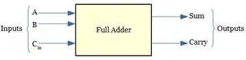
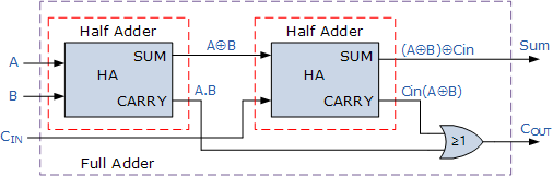
Full Adder:
Digital electronics form the cornerstone of modern computing and information processing systems. Among the fundamental building blocks of digital circuits is the full adder, a crucial component in arithmetic and logic operations. In this comprehensive overview, we will delve into the intricacies of the full adder, exploring its operations and implementation using NAND gates.
Introduction:
The full adder is a combinational logic circuit that adds three binary digits, A, B, and \(C_{in}\) (carry-in), to produce two outputs: Sum (\(S\)) and Carry-out (\(C_{out}\)). It is an essential element in multi-bit arithmetic operations, making it a crucial part of microprocessors and other digital systems.
Full Adder Truth Table:
To understand the functioning of a full adder, we begin by examining its truth table. The table lists all possible combinations of inputs (A, B, \(C_{in}\)) and corresponding outputs (\(S\), \(C_{out}\)). The full adder truth table consists of eight rows, each representing a unique input configuration.
| A | B | \(C_{in}\) | \(S\) | \(C_{out}\) |
|---|---|---|---|---|
| 0 | 0 | 0 | 0 | 0 |
| 0 | 0 | 1 | 1 | 0 |
| 0 | 1 | 0 | 1 | 0 |
| 0 | 1 | 1 | 0 | 1 |
| 1 | 0 | 0 | 1 | 0 |
| 1 | 0 | 1 | 0 | 1 |
| 1 | 1 | 0 | 0 | 1 |
| 1 | 1 | 1 | 1 | 1 |
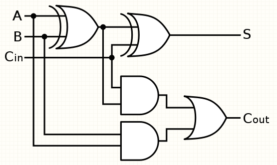
Full Adder Operations:
The full adder performs three main operations during the addition process: adding the individual bits (A and B), considering the carry-in (\(C_{in}\)), and generating the carry-out (\(C_{out}\)).
Bit Addition (Sum, \(S\)): The XOR operation (exclusive OR) is used to add the individual bits A and B. XOR produces an output of '1' when the inputs are different and '0' when they are the same. This operation captures the essence of adding two binary numbers without considering the carry.
Carry Generation (Carry-out, \(C_{out}\)): The AND operation is employed to determine when a carry-out occurs. If both inputs A and B are '1,' an AND gate will output '1,' indicating that a carry must be propagated to the next bit.
Carry Propagation (\(C_{in}\)): The carry-in (\(C_{in}\)) represents any carry generated from the addition of previous bits in multi-bit operations. If \(C_{in}\) is '1,' it indicates an additional bit must be added to the sum to account for the carry.
Full Adder Implementation Using NAND Gates:
NAND gates are versatile components that can be combined to create various digital logic functions. Here, we illustrate the construction of a full adder using NAND gates, demonstrating how this fundamental circuit can be realized in practice.
The NAND gate performs the logical negation of an AND gate. It produces an output of '0' only when both inputs are '1,' otherwise, it outputs '1.'
1. Implementing Sum (\(S\)):
To construct the Sum output (\(S\)) of the full adder, we need to perform an XOR operation between A, B, and \(C_{in}\). Here is how it is achieved using NAND gates:
- Connect A and B to two separate NAND gates (N1 and N2) acting as inverters.
- Connect A and B to a third NAND gate (N3) to produce A NAND B.
- Connect the outputs of N1, N2, and N3 to a fourth NAND gate (N4) to obtain (A NAND B) NAND (A NAND B) NAND (A NAND B).
- Connect \(C_{in}\) to a fifth NAND gate (N5) acting as an inverter.
- Connect the output of N4 and N5 to a sixth NAND gate (N6) to get [((A NAND B) NAND (A NAND B) NAND (A NAND B)) NAND \(C_{in}\)].
The output of N6 represents the Sum (\(S\)) of the full adder.
2. Implementing Carry-out (\(C_{out}\)):
The Carry-out (\(C_{out}\)) is determined by the AND operation between A, B, and \(C_{in}\). This can be realized using NAND gates as follows:
- Connect A, B, and \(C_{in}\) to three separate NAND gates (N7, N8, and N9) acting as inverters.
- Connect the outputs of N7, N8, and N9 to a fourth NAND gate (N10) to obtain [(A NAND A) NAND (B NAND B) NAND (\(C_{in}\) NAND \(C_{in}\))].
- Connect the output of N10 to a fifth NAND gate (N11) acting as an inverter.
- Connect the output of N11 to a sixth NAND gate (N12) to get the final output, which represents the Carry-out (\(C_{out}\)).
Half Subtractor:
Digital electronics is a branch of electronics that deals with the manipulation of discrete signals, represented by binary numbers (0s and 1s). One of the fundamental operations in digital electronics is subtraction, which is essential for arithmetic and logic operations. A half subtractor is a combinational logic circuit that performs the subtraction of two binary digits, providing both the difference and borrow outputs. In this article, we will delve into the working principles, circuit design, truth table, and applications of a half subtractor.
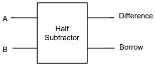
Introduction:
A half subtractor is designed to subtract two single binary digits, often referred to as the minuend (A) and the subtrahend (B), producing two outputs: the difference (D) and the borrow (\(B_{out}\)). The borrow output indicates whether a borrow is required during subtraction.
Truth Table and Logic Equations:
The truth table of a half subtractor lists all possible input combinations and their corresponding outputs. There are four possible input combinations for a half subtractor:
| A | B | D | \(B_{out}\) |
|---|---|---|---|
| 0 | 0 | 0 | 0 |
| 0 | 1 | 1 | 1 |
| 1 | 0 | 1 | 0 |
| 1 | 1 | 0 | 0 |
From the truth table, we can derive the logic equations for the difference (D) and borrow (\(B_{out}\)) outputs:
Difference (D) = B + A Borrow (\(B_{out}\)) = B
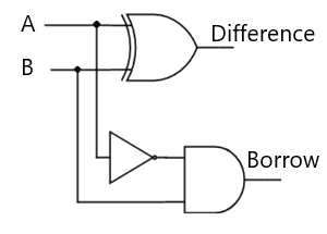
Half Subtractor Circuit Design:
The half subtractor can be implemented using logic gates such as AND, OR, and NOT gates. The logic diagram of a half subtractor consists of these basic gates interconnected to achieve the subtraction operation.
AND Gate: The AND gate takes two binary inputs and produces an output only when both inputs are high (1). In the context of a half subtractor, an AND gate is used to generate the borrow output.
OR Gate: The OR gate produces an output when at least one of its inputs is high (1). In the half subtractor circuit, OR gates are used to determine the difference output.
NOT Gate: The NOT gate, also known as an inverter, produces the logical complement of its input. It is used to negate the subtrahend (B) input to obtain the inverted B input, which is essential for calculating the difference.
Half Subtractor Operation:
The operation of a half subtractor is explained using an example: Suppose we want to subtract 1 (B) from 0 (A).
Step 1: A = 0, B = 1
Step 2: Calculate the borrow (\(B_{out}\)) using the logic equation: \(B_{out}\) = B = 0 × 1 = 0
Step 3: Calculate the difference (D) using the logic equation: D = B + A = 0 × 1 + 0 × 1 = 0
In this example, the difference (D) is 0, indicating that 0 - 1 results in 0. The borrow (\(B_{out}\)) is also 0, indicating that no borrow is required.
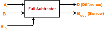
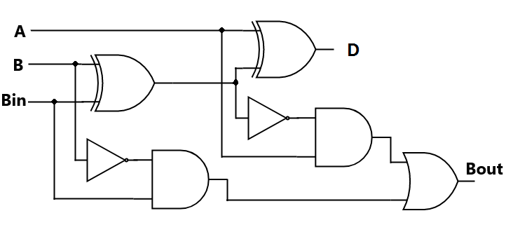
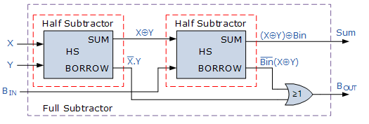
Full Subtractor:
Full subtractor is a combinational circuit used to subtract three binary digits, taking into account the borrow from the previous stage.
Introduction to Full Subtractor:
A full subtractor is a logical circuit that takes three binary inputs: the minuend (A), the subtrahend (B), and a borrow input (\(B_{in}\)). It produces two outputs: the difference (\(Diff\)) and a borrow output (B_{out}). The borrow input (\(B_{in}\)) is the carry generated by the subtraction of the previous stage. The full subtractor circuit is crucial for performing binary subtraction in multi-bit systems.
Full Subtractor Operations:
The full subtractor performs three main operations: subtracting binary digits, handling borrow inputs, and generating outputs. Let's break down these operations step by step:
- Subtracting Binary Digits: The core operation of a full subtractor is the subtraction of two binary digits (A and B). There are four possible scenarios for these two input bits:
- A = 0, B = 0: This results in \(Diff\) = 0 and \(B_{out}\) = 0.
- A = 0, B = 1: In this case, \(Diff\) = 1 if \(B_{in}\) = 0, and \(Diff\) = 0 if \(B_{in}\) = 1. \(B_{out}\) is set to 1 in both cases.
- A = 1, B = 0: Here, \(Diff\) = 1 if \(B_{in}\) = 1, and \(Diff\) = 0 if \(B_{in}\) = 0. \(B_{out}\) is set to 0 in both cases.
- A = 1, B = 1: This leads to \(Diff\) = 0 and \(B_{out}\) = 0 if \(B_{in}\) = 1. \(Diff\) = 1 and \(B_{out}\) = 1 if \(B_{in}\) = 0.
Handling Borrow Inputs: The borrow input (\(B_{in}\)) is essential for handling situations where borrowing is required from the previous stage. It enables the subtraction of more significant bits that depend on the result of the lower-order bits. If \(B_{in}\) = 1, it indicates that a borrow is required from the previous stage, influencing the subtraction process.
Generating Outputs: The full subtractor produces two main outputs: the difference (\(Diff\)) and the borrow output (B_{out}). \(Diff\) represents the result of the binary subtraction operation between A and B, along with the borrow input \(B_{in}\). \(B_{out}\) indicates whether borrowing occurred during the subtraction process and is used as a carry for the subsequent stages.
Truth Table for Full Subtractor:
The truth table for a full subtractor outlines all possible combinations of inputs and their corresponding outputs. Considering the inputs A, B, and \(B_{in}\), and the outputs \(Diff\) and \(B_{out}\), the truth table for a full subtractor is as follows:
| A | B | \(B_{in}\) | \(Diff\) | \(B_{out}\) |
|---|---|---|---|---|
| 0 | 0 | 0 | 0 | 0 |
| 0 | 0 | 1 | 1 | 1 |
| 0 | 1 | 0 | 1 | 1 |
| 0 | 1 | 1 | 0 | 1 |
| 1 | 0 | 0 | 0 | 0 |
| 1 | 0 | 1 | 0 | 0 |
| 1 | 1 | 0 | 1 | 0 |
| 1 | 1 | 1 | 0 | 1 |
In the truth table, each row corresponds to a unique combination of input values, and the corresponding outputs \(Diff\) and \(B_{out}\) are provided. This table encapsulates the full subtractor's behavior in response to various input scenarios.
Binary Adder-Subtractor
The binary adder-subtractor circuit is an essential building block in digital systems, facilitating both addition and subtraction operations within a single integrated circuit.
Binary Adder-Subtractor Circuit:
A binary adder-subtractor circuit combines the functionalities of an adder and a subtractor into a single unit, allowing for versatile computation. This circuit is designed to handle two binary numbers, performing either an addition or a subtraction operation based on control inputs.
Operations of the Binary Adder-Subtractor Circuit
The binary adder-subtractor circuit performs two primary operations: addition and subtraction. It is equipped with a control input that determines whether the circuit should perform an addition or subtraction operation. This control input is typically denoted as the "subtract" or "Borrow-In" (\(B_{in}\)) signal. When the \(B_{in}\) signal is set to 0, the circuit performs an addition, and when it is set to 1, the circuit performs subtraction.

Binary Addition Operation:
Binary addition involves the process of adding two binary numbers, similar to the conventional decimal addition. The binary adder-subtractor circuit performs this operation by considering individual bits of the numbers along with a carry input. The circuit follows a cascading structure, where each stage handles a pair of bits from the input numbers along with the carry generated by the previous stage. The operation at each stage includes three inputs: A, B, and the carry from the previous stage (\(C_{in}\)), and two outputs: the sum (S) and the carry-out (\(C_{out}\)) for the next stage.
The sum (\(S\)) at each stage is computed using the XOR gate, while the carry-out (\(C_{out}\)) is determined using the AND and XOR gates. The carry-in (\(C_{in}\)) for the least significant bit (LSB) stage is typically set to 0. The carry-out from the most significant bit (MSB) stage is considered the final carry-out of the entire addition operation.
Binary Subtraction Operation:
Binary subtraction, when performed manually, involves borrowing from higher-order bits to perform the subtraction of lower-order bits. The binary adder-subtractor circuit automates this process using the control input \(B_{in}\). When the \(B_{in}\) input is set to 1, the circuit performs subtraction. To achieve this, the two's complement method is utilized. The two's complement of a binary number is obtained by inverting its bits (changing 0s to 1s and vice versa) and adding 1 to the result.
When subtracting a binary number B from another binary number A, the circuit computes the sum of A and the two's complement of B. By using the two's complement, subtraction is transformed into addition, which can be handled by the same binary adder circuit. The final output is then corrected by discarding the carry-out from the MSB stage and considering it as an overflow indicator.
Truth Table of the Binary Adder-Subtractor Circuit:
The truth table of a binary adder-subtractor circuit outlines its behavior based on various inputs. The circuit has three primary inputs: A, B, and \(B_{in}\) (the control input), and two outputs: \(S\) (sum) and (\(C_{out}\)) (carry-out). Since the control input \(B_{in}\) determines whether the circuit performs addition or subtraction, the truth table can be divided into two parts: one for addition (\(B_{in}\) = 0) and another for subtraction (\(B_{in}\) = 1).
Truth Table for Addition (\(B_{in}\) = 0):
| A | B | \(B_{in}\) | \(S\) | \(C_{out}\) |
|---|---|---|---|---|
| 0 | 0 | 0 | 0 | 0 |
| 0 | 1 | 0 | 1 | 0 |
| 1 | 0 | 0 | 1 | 0 |
| 1 | 1 | 0 | 0 | 1 |
Truth Table for Subtraction (\(B_{in}\) = 1):
| A | B | \(B_{in}\) | \(S\) | \(C_{out}\) |
|---|---|---|---|---|
| 0 | 0 | 1 | 0 | 0 |
| 0 | 1 | 1 | 1 | 1 |
| 1 | 0 | 1 | 1 | 0 |
| 1 | 1 | 1 | 0 | 0 |
The truth table illustrates the outcomes of the binary adder-subtractor circuit based on various input combinations. When the control input \(B_{in}\) is set to 0, the circuit performs binary addition, while setting \(B_{in}\) to 1 results in binary subtraction.