Registers
A register is a very important digital building block. A data register is often used to momentarily store binary information appearing at the output of an encoding matrix. A register might be used to accept input data from an alphanumeric keyboard and then present this data at the input of a microprocessor chip. Similarly, registers are often used to momentarily store binary data at the output of a decoder. For instance, a register could be used to accept output data from a microprocessor chip and then present this data to the circuitry used to drive the display on a CRT screen.
A binary register also forms the basis for some very important arithmetic operations. For example, the operations of complementation, multiplication, and division are frequently implemented by means of a register. A shift register can also be connected to form a number of different types of counters. Shift registers as sequence generator and sequence detector and also as parallel to serial converters offers very distinct advantages.
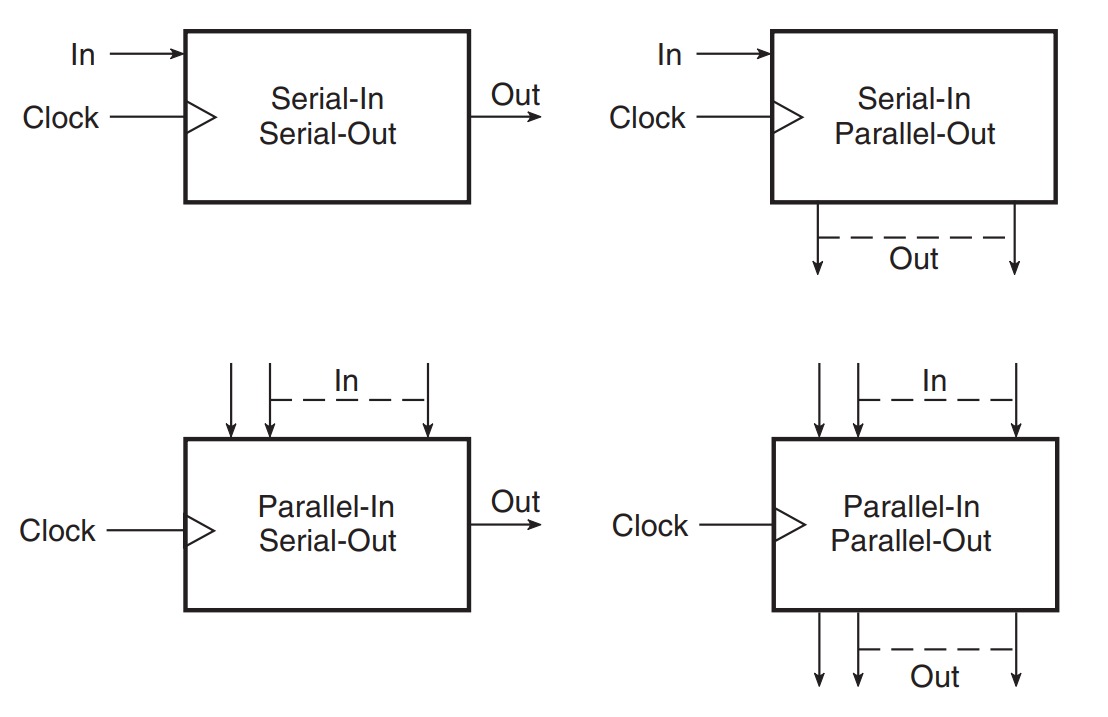
A register is simply a group of flip-flops that can be used to store a binary number. "There must be one flip-flop for each bit in the binary number. For instance, a register used to store an 8-bit binary number must have eight flip-flops. Naturally the flip-flops must be connected such that the binary number can be entered (shifted) into the register and possibly shifted out. A group of flip-flops connected to provide either or both of these functions is called a shift register. The bits in a binary number can be moved from one place to another in either of two ways. The first method involves shifting the data 1 bit at a time in a serial fashion, beginning with either the most significant bit (MSB) or the least significant bit (LSB) referred to as serial shifting. The second method involves shifting all the data bits simultaneously and is referred to as parallel shifting. There are two ways to shift data into a register (serial or parallel) and similarly two ways to shift the data out of the register. This leads to the construction of four basic register types.
- Serial in-serial out
- Serial in-parallel out
- Parallel in-serial out
- Parallel in-parallel out
Serial in-serial out
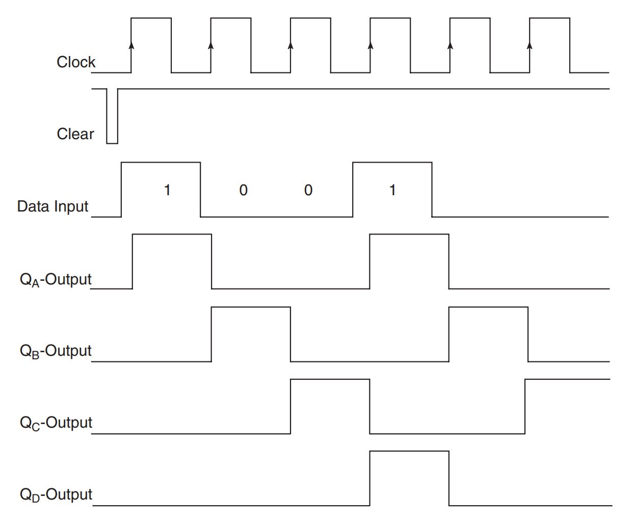
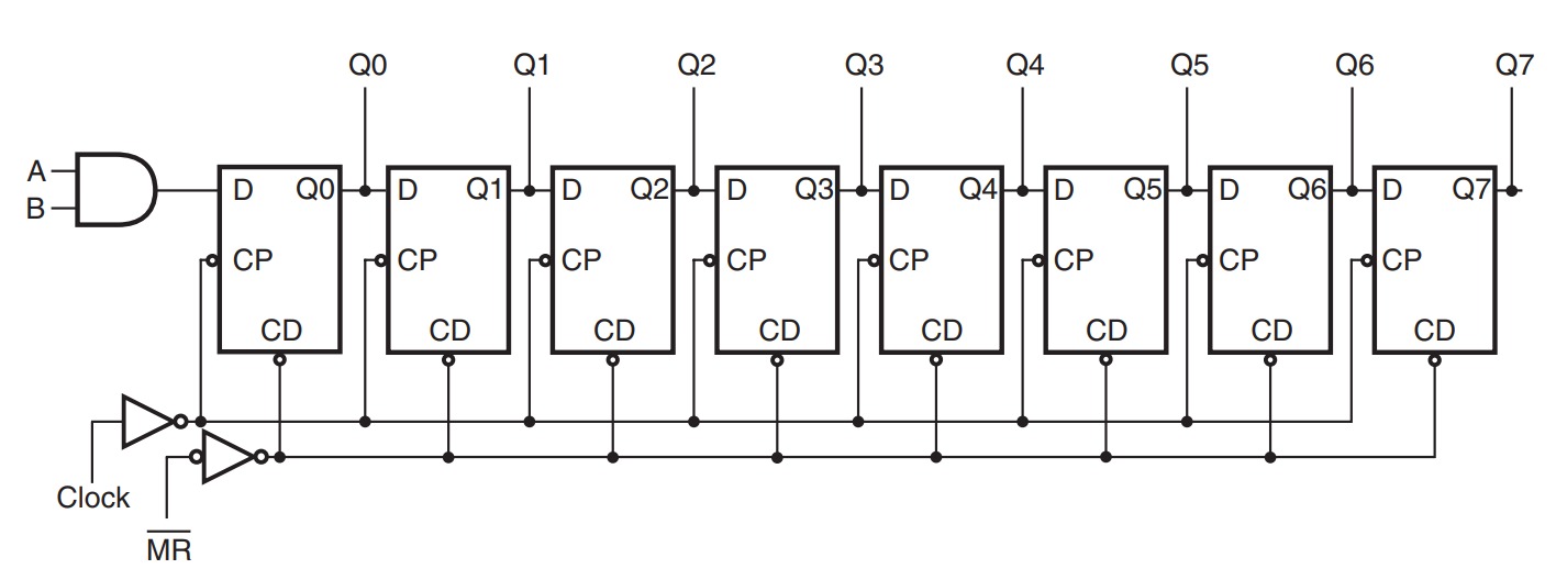
Four D flip-flops connected as shown in Fig. 9.2a forming 4-bit shift register. A common clock provides trigger at its negative edge to all the flip-flops. As output of one D flip-flop is com1ected to input of the next at every Clock trigger data stored in one flip-flop is transferred to the next.

Serial in-parallel out
The second type of register which shifts data in serially but shifted out in parallel. In order to shift the data out in parallel, it is simply necessary to have all the data bits available as outputs at the same time. This is easily accomplished by connecting the output of each flip-flop to an output pin.
The serial data is connected to A; then B can be used as a control line. B is Held High The NAND gate is enabled and the serial input data passes through the NAND gate inverted. The input data is shifted serially into the register. B is Held Low The NAND-gate output is forced high, the input data stream is inhibited, and the next positive clock transition will shift a O into the first flip-flop. Each succeeding positive clock transition will shift another O into the register. After eight clock pulses, the register will be full of zeros!
Parallel In and Serial Out

Bi-directional Shift register
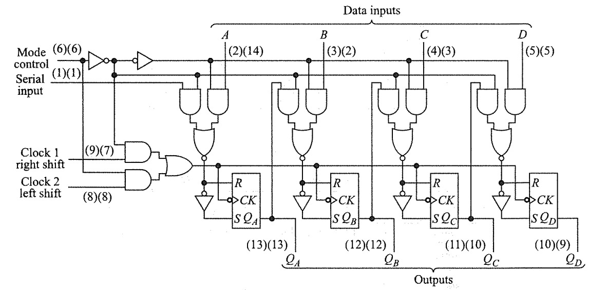
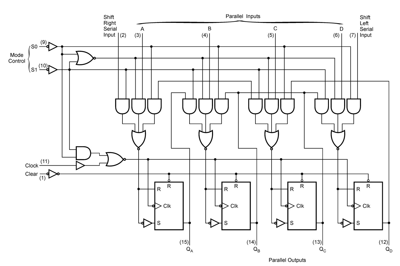
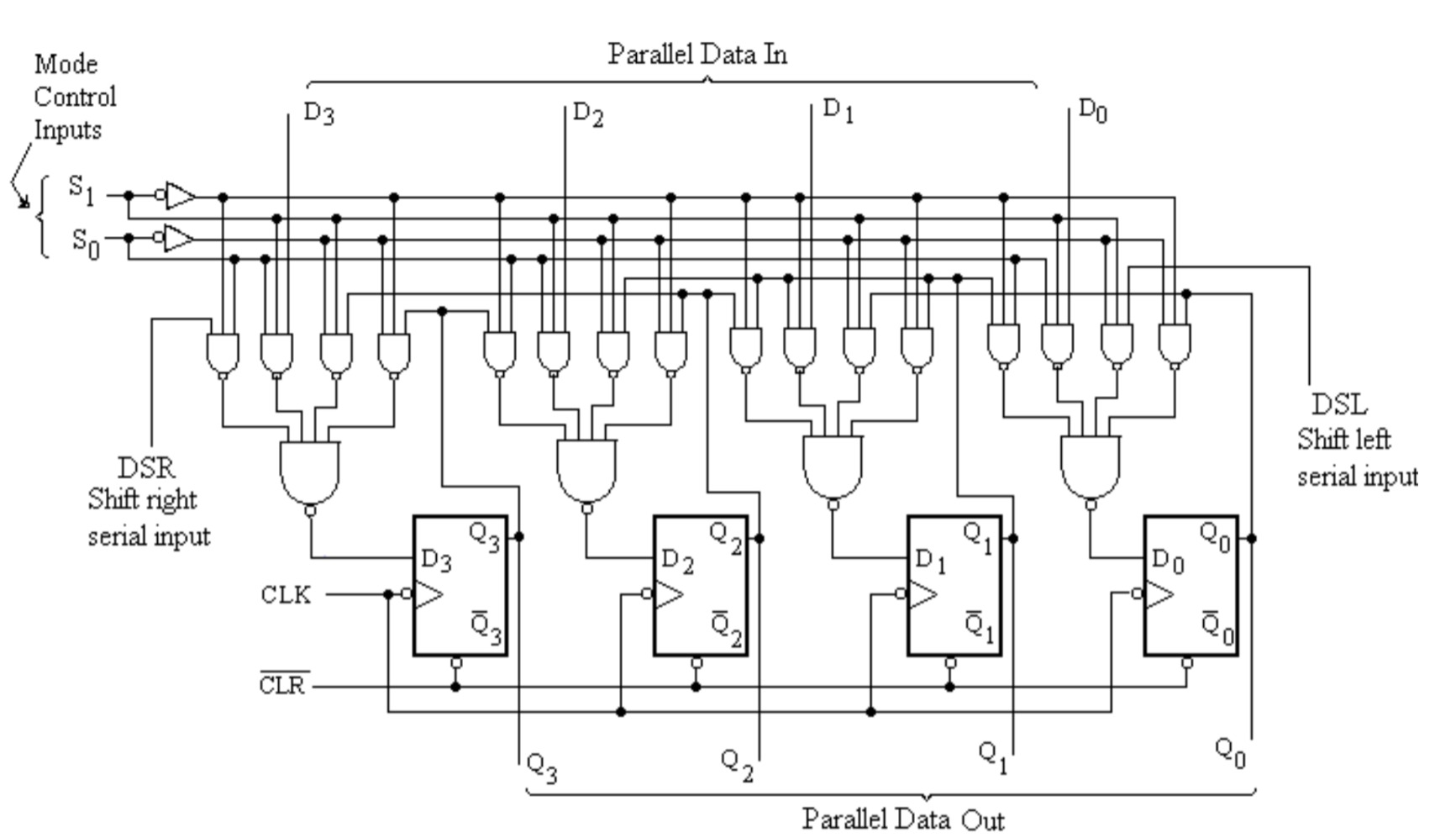
Universal Shift Register