Analog to Digital converter
Generally, the information to be processed by the digital systems is analog. So, before applying such signals to digital systems, it is necessary to convert the signal into its equivalent digital form. The method with the help of which analog signal may be converted to digital form is known as digital to analog (D/A) converter. The A/D converter is more complex and difficult than the D/A converter. The following are the different methods for A/D converter.
- (i) Simultaneous A/D converter
- (ii) Successive approximation D/A converter
- (iii) Counter or Digital Ramp type A/ D converter
- (iv) Single slope D/A converter
- (v) Dual slope D/A converter
Simultaneous A/D converter
This is the fastest and simplest method of converting analog signals to digital ones. It utilizes parallel differential comparators; the input analog voltage is compared by these comparators with known voltages called reference voltages. The comparators give the low output (logic \(0\)) when the input is less than the reference voltage and give the high output (logic \(1\)) when the input analog voltage exceeds the reference voltage. This method of conversion is also called a Flash or parallel-type A/D converter.
For converting analog voltage ranging between 0 to \(V\) volts into two-bit digital output, three comparators (generally \(2^n – 1\) comparators where \(n\) in the number of bits) are required. The input analog voltage is converted to the 4 (in general \(2^n\)) equal regions, as shown in the table. If the analog voltage lies in the first region, then the binary bits (\(b_1\), \(b_0\)) are \(00\). Similarly to the second, third, and fourth regions, the binary bits are \(01\), \(10\), and \(11\), respectively.
| \(V\) volts | \(IV\) Region | \(b_{1}b_{1}=11\) |
| \(3V/4\) volts | \(III\) Region | \(b_{1}b_{0}=10\) |
| \(V/2\) volts | \(II\) Region | \(b_{0}b_{1}=01\) |
| \(V/4\) volts | \(I\) Region | \(b_{0}b_{0}=00\) |
| \(0\) volts | --- | --- |
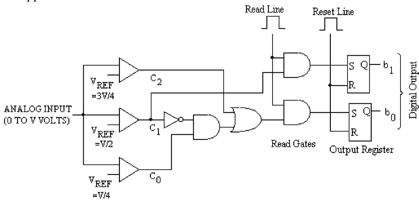
The reference voltages to the three comparators \(C_0\), \(C_1\), \(C_2\) should be \(V/4\), \(V/2\), and \(3V/4\), respectively, as shown in the table. The output of the three comparators should be connected to the logic gates to produce the desired binary output. The read gates and output registers are used to read the digital output.
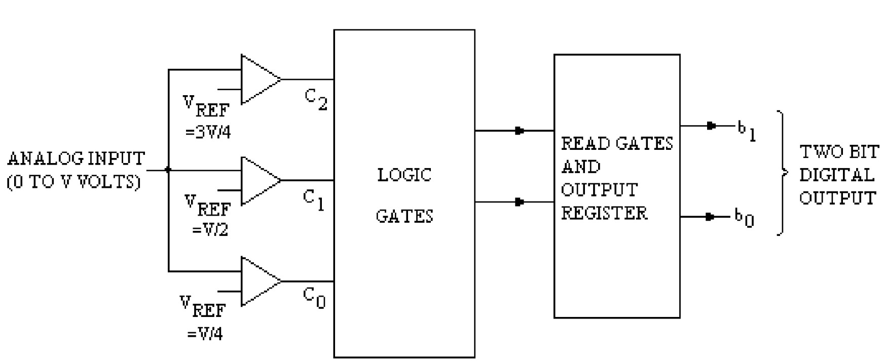
Referring to the figures, if the input analog voltage exceeds the reference voltage to any comparator, the comparator gives high output (logic \(1\)); if, on the other hand, the input analog voltage is less than the reference voltage of the comparator, it gives low output (logic \(0\)). In this way, if all the comparators give low output, the analog input voltage must be between \(0\) and \(V/4\) volts (\(I\) region), and the digital binary output should be \(00\). If the \(C_0\) is high and \(C_1\) and \(C_2\) are low, the input must be between \(V/4\) and \(V/2\) volts (\(II\) regions), and the digital binary output should be \(01\). If \(C_0\) and \(C_1\) are high and \(C_2\) is low, the input must be between \(V/2\) and \(3V/4\) volts (\(III\) regions), and the digital binary output should be \(10\). Finally, if all the comparators give high outputs, the input must lie between \(3V/4\) and \(V\) volts (\(IV\) regions), and the digital binary output should be \(11\). The table summarizes the outputs of the comparators.
| Input Voltage | \(C_{2}\) | \(C_{1}\) | \(C_{0}\) | \(b_{1}\) | \(b_{0}\) |
|---|---|---|---|---|---|
| \(0\) to \(V/4\) | 0 | 0 | 0 | 0 | 0 |
| \(V/4\) to \(V/2\) | 0 | 0 | 1 | 0 | 1 |
| \(V/2\) to \(3V/4\) | 0 | 1 | 1 | 1 | 0 |
| \(3V/4\) to \(V\) | 1 | 1 | 1 | 1 | 1 |
By drawing the \(K\)–maps (figure), the expressions for \(b_0\) and \(b_1\) are obtained as \(b_1=C_1\) and \(b_0 = \overline{C_0}C_1+C_2\)
| \(\diagdown\) |
| \(\overline{C_{2}}\overline{C_{1}}\) | \(\overline{C_{2}}C_{1}\) | \(C_{2}C_{1}\) | \(C_{2}\overline{C_{1}}\) |
| \(\overline{C_{0}}\) |
| \(C_{0}\) |
| 0 | X | X | X |
| 0 | 1 | 1 | X |
| \(b_{1}=\) |
| \(C_{1}\) |
| \(\diagdown\) |
| \(\overline{C_{2}}\overline{C_{1}}\) | \(\overline{C_{2}}C_{1}\) | \(C_{2}C_{1}\) | \(C_{2}\overline{C_{1}}\) |
| \(\overline{C_{0}}\) |
| \(C_{0}\) |
| 0 | X | X | X |
| 1 | 0 | 1 | X |
| \(b_{0}=\) |
| \(\overline{C_{0}}C_{1}+C_{2}\) |
As shown in the figure, these expressions may be realized using the gates. The output may be reset by applying a high signal to the reset line, and reading the data at a high signal is applied to the read line.
For converting analog input voltage (\(0\) to \(V\) volts) into three-bit binary output, we proceed in a similar method to the two-bit output. For the three-bit outputs, the input voltages are divided into \(8\) (as \(2^3 = 8\)) equal regions, and \(7\) (as \(2^3-1 = 7\)) comparators are to be used. So, the logic circuit to be designed should have seven inputs (output of the seven comparators) and three outputs. The output of comparators and the corresponding binary output are shown in the table.
| Input Voltage | \(C_{6}\) | \(C_{5}\) | \(C_{4}\) | \(C_{3}\) | \(C_{2}\) | \(C_{1}\) | \(C_{0}\) | \(b_{2}\) | \(b_{1}\) | \(b_{0}\) |
|---|---|---|---|---|---|---|---|---|---|---|
| \(0\) to \(V/8\) | 0 | 0 | 0 | 0 | 0 | 0 | 0 | 0 | 0 | 0 |
| \(V/8\) to \(V/4\) | 0 | 0 | 0 | 0 | 0 | 0 | 1 | 0 | 0 | 1 |
| \(V/4\) to \(3V/8\) | 0 | 0 | 0 | 0 | 0 | 1 | 1 | 0 | 1 | 0 |
| \(3V/8\) to \(V/2\) | 0 | 0 | 0 | 0 | 1 | 1 | 1 | 0 | 1 | 1 |
| \(V/2\) to \(5V/8\) | 0 | 0 | 0 | 1 | 1 | 1 | 1 | 1 | 0 | 0 |
| \(5V/8\) to \(3V/4\) | 0 | 0 | 1 | 1 | 1 | 1 | 1 | 1 | 0 | 1 |
| \(3V/4\) to \(7V/8\) | 0 | 1 | 1 | 1 | 1 | 1 | 1 | 1 | 1 | 0 |
| \(7V/8\) to \(V\) | 1 | 1 | 1 | 1 | 1 | 1 | 1 | 1 | 1 | 1 |
The expressions of the output bits can easily be obtained by examining the table.
The bit \(b_2\) gives the high output whenever the output of the comparator \(C_3\) is high. The bit \(b_1\) is high whenever the output of comparator \(C_1\) is high, and the output of \(C_3\) is low, or whenever the output of comparator \(C_5\) is high. Similarly, the expression for bit \(b_0\) can be obtained. All the boolean expressions are consolidated below:
\[ b_{0}=C_{0}\overline{C_{1}}+C_{2}\overline{C_{3}}+C_{4}\overline{C_{5}}+C_{6} \] \[ b_{1}=C_{1}\overline{C_{3}}+C_{5} \] \[ b_{2}=C_{3} \]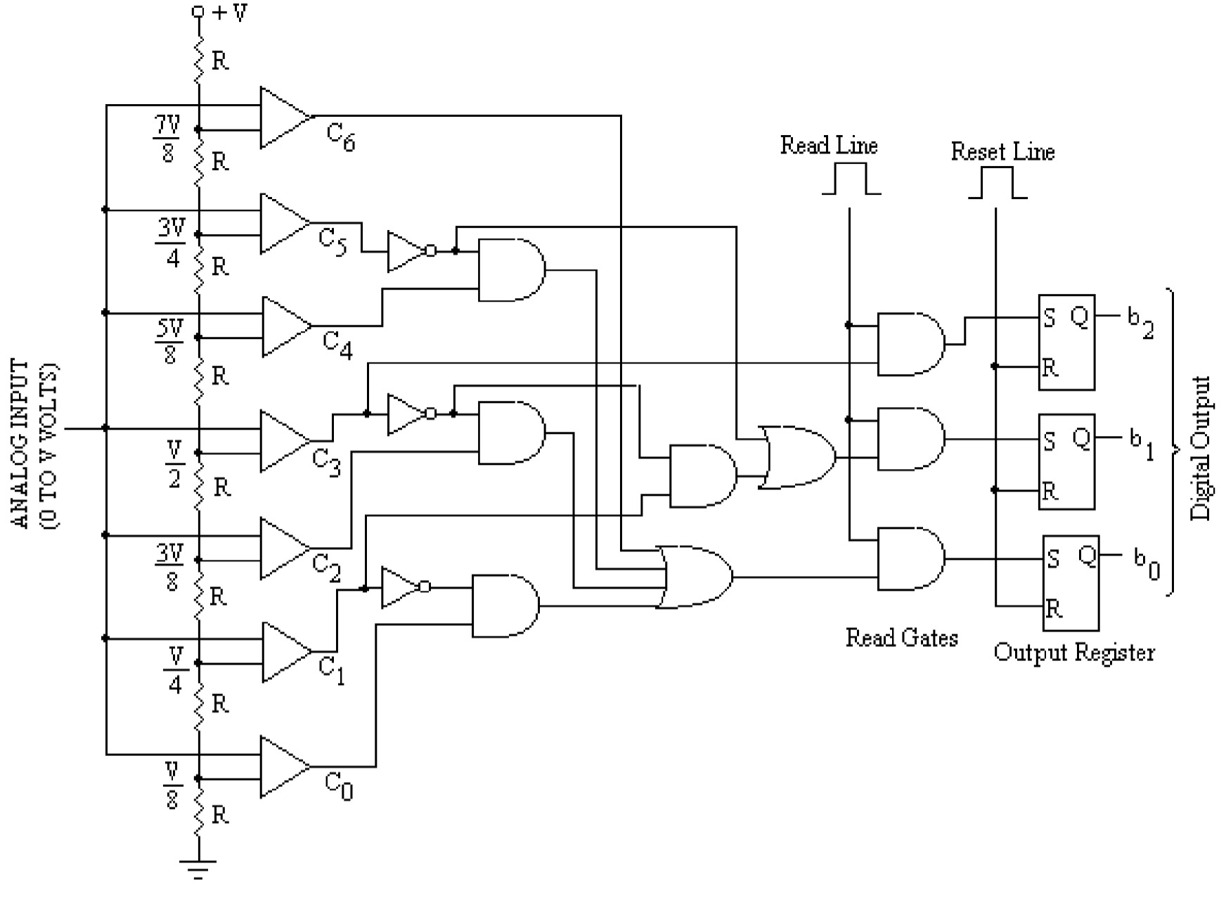
As shown in the figure, these expressions may be realized using the gates. The output may be reset by applying a high signal to the reset line, and reading the data at a high signal is applied to the read line. The design of a simultaneous A/D converter is quite straightforward and relatively easy to understand. However, the design becomes complicated as the number of bits increases since the number of comparators to be used increases drastically. This method has the highest speed of conversion.
Successive approximation D/A converter
Simultaneous A/D converter has a very fast conversion time but becomes unwieldy when the required digital bits are more. The successive approximation method is the most useful and commonly used method. The block diagram four-bit successive approximation A/D converter is shown in the figure. It consists of a D/A converter, successive approximation register (SAR), and a comparator. The basic principle of this A/D converter is as follows:
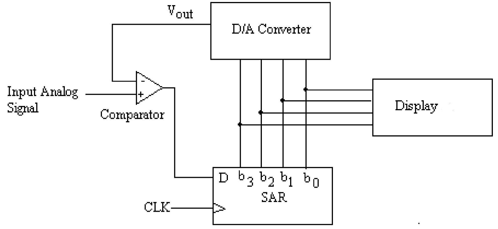
In this type of converter, the bits of the D/A converter are enabled one by one, starting with the most significant bit (MSB). The analog output of the D/A converter corresponding to the enabled bit is compared with the input analog voltage. The comparator gives the output low if the input analog voltage is less than the output of the D/A converter, and it gives the high out if the input analog voltage is more than the output of the D/A converter. The low output of the comparator resets the corresponding bit of SAR. On the other hand, if the comparator's output is high, then that bit is retained in SAR. In this way, the output of the D/A converter is compared with the input voltage for all the bits, starting with the most significant bit. Thus, the successive approximation method approximates the analog voltage bit by bit, starting with MSB. This process is shown in the figure.
To understand the operation of this type of A/D converter, we will take a specific example of a four-bit conversion. Figure (a through d) shows a given analog input voltage's step–by–step conversion (say \(6\) volts). It is further assumed that the D/A converter has the following output characteristics:
- \(V_{out} = 8\) volts for bit \(3\) (MSB or \(b_3\))
- \(V_{out} = 4\) volts for bit \(2\) (2nd MSB or \(b_2\))
- \(V_{out} = 2\) volts for bit \(1\) (3rd MSB or \(b_1\))
- \(V_{out} = 1\) volt for bit \(0\) (LSB or \(b_0\))
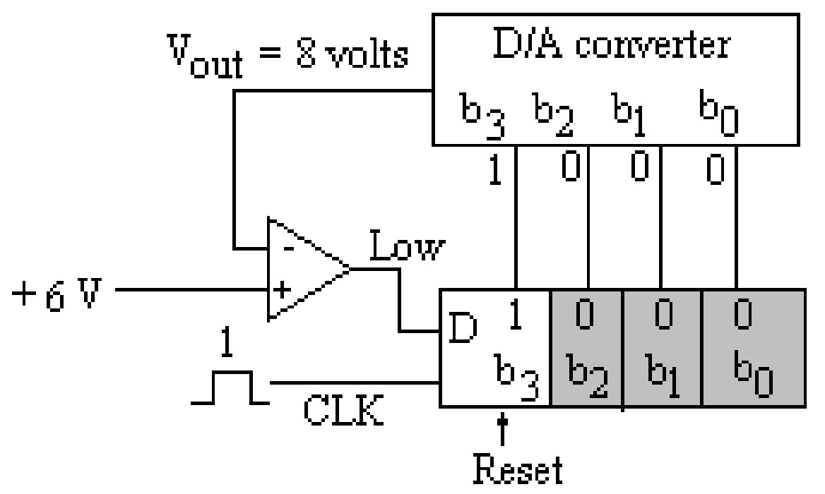
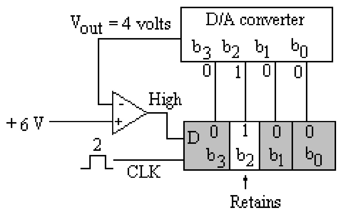
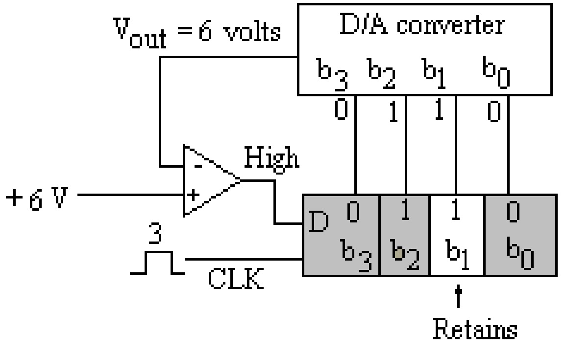
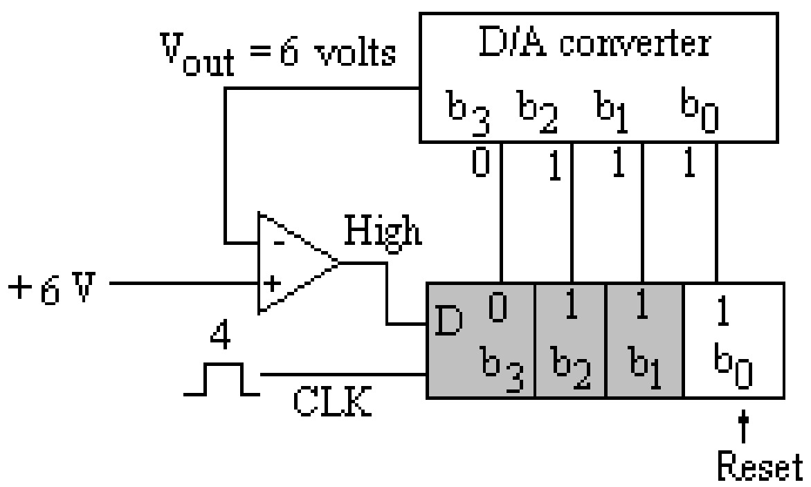
It is clear from these figures that after completing the conversion cycle. The binary code \(0110\) is retained in SAR, which is the binary value of the input voltage (\(6\) volts). It is finally displayed on the display devices.
Counter or Digital Ramp type A/ D converter
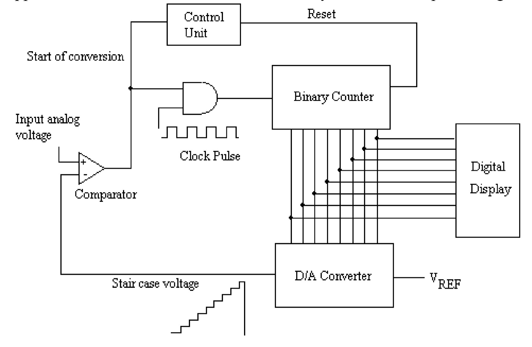
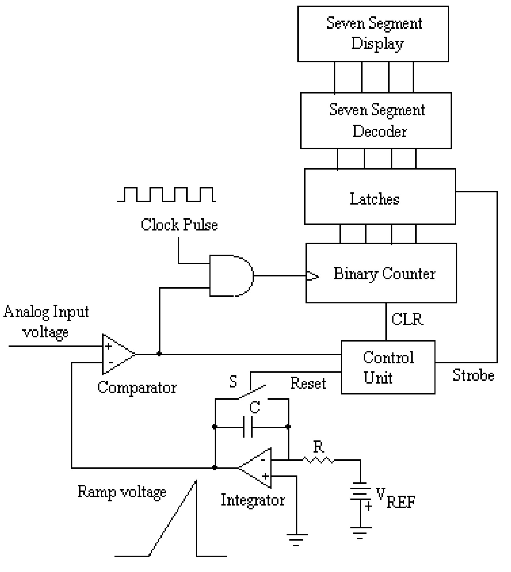
Another method of converting the analog signal to a digital one is the counter or digital ramp type A/D converter, which utilizes a binary counter to count a continuous pulse of standard width and height from a clock. The standard clock pulses are passed through a gate that is open for some time to allow these pulses to go to the input of the counter. Normally, the gate is closed, and a staircase voltage is initiated as soon as the start signal is applied. This voltage is increased linearly with the increase of the binary counts in the counter. The gate remains open when the linear staircase voltage equals the input analog voltage. The counter records the number of clock pulses proportional to the input analog voltage.
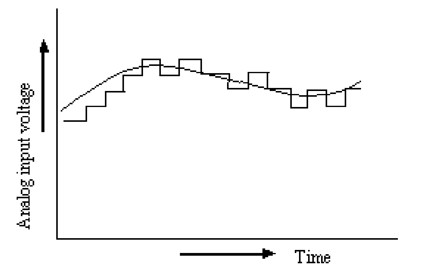
Figure shows the schematic diagram of this type of A/D converter. To be converted to its equivalent digital output, the analog signal is applied to one input of an operational amplifier as a comparator. When a start of conversion pulse is applied to the control unit, it resets the binary counter and opens the gate. The counter starts counting the clock pulses of standard width and height. The output of the counter is fed to a D/A converter, which produces an analog output (staircase voltage) in response to the digital signal (output of the counter) as its input. This analog output voltage is fed to the reference input of the comparator. So long as the input analog signal is more significant than the staircase voltage, the comparator provides the high output to the gate, the gate remains open, and the clock pulses are allowed to reach the input of the counter. The counter counts these pulses, thus continuously increasing the digital output. When the analog output of the D/A converter (staircase voltage) exceeds the input analog voltage, the comparator provides a low output, disabling the gate, and the counter stops counting. The binary number stored in the counter represents the digital output voltage corresponding to the input analog voltage. The digital output is displayed on the display devices.
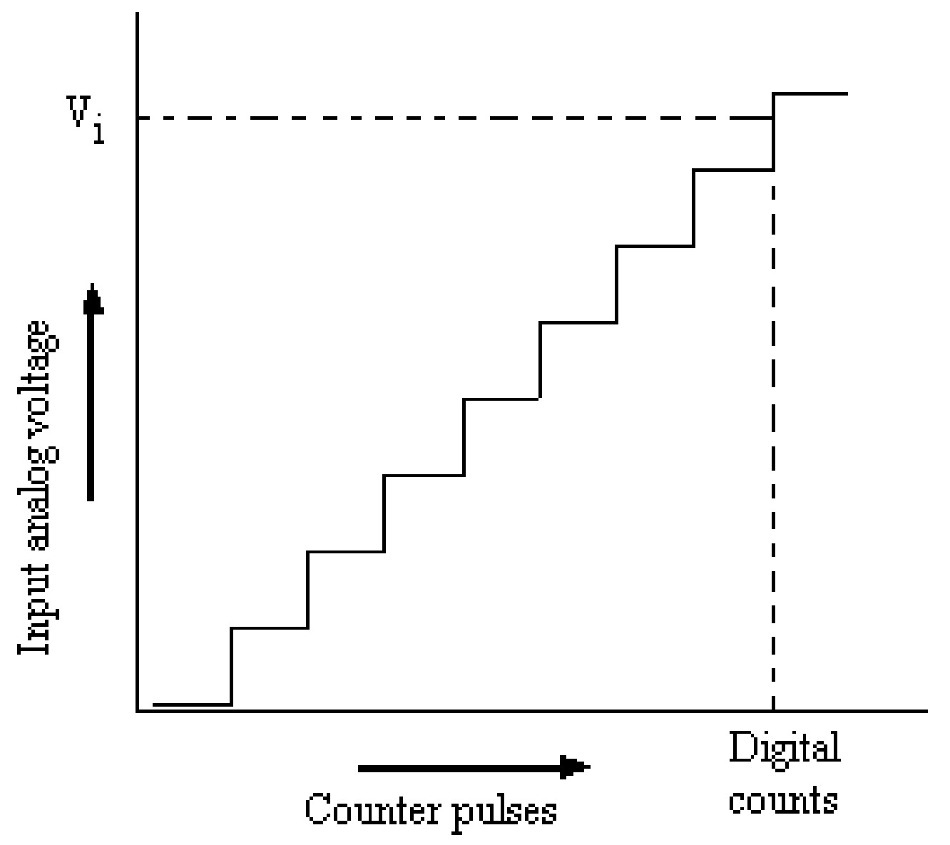
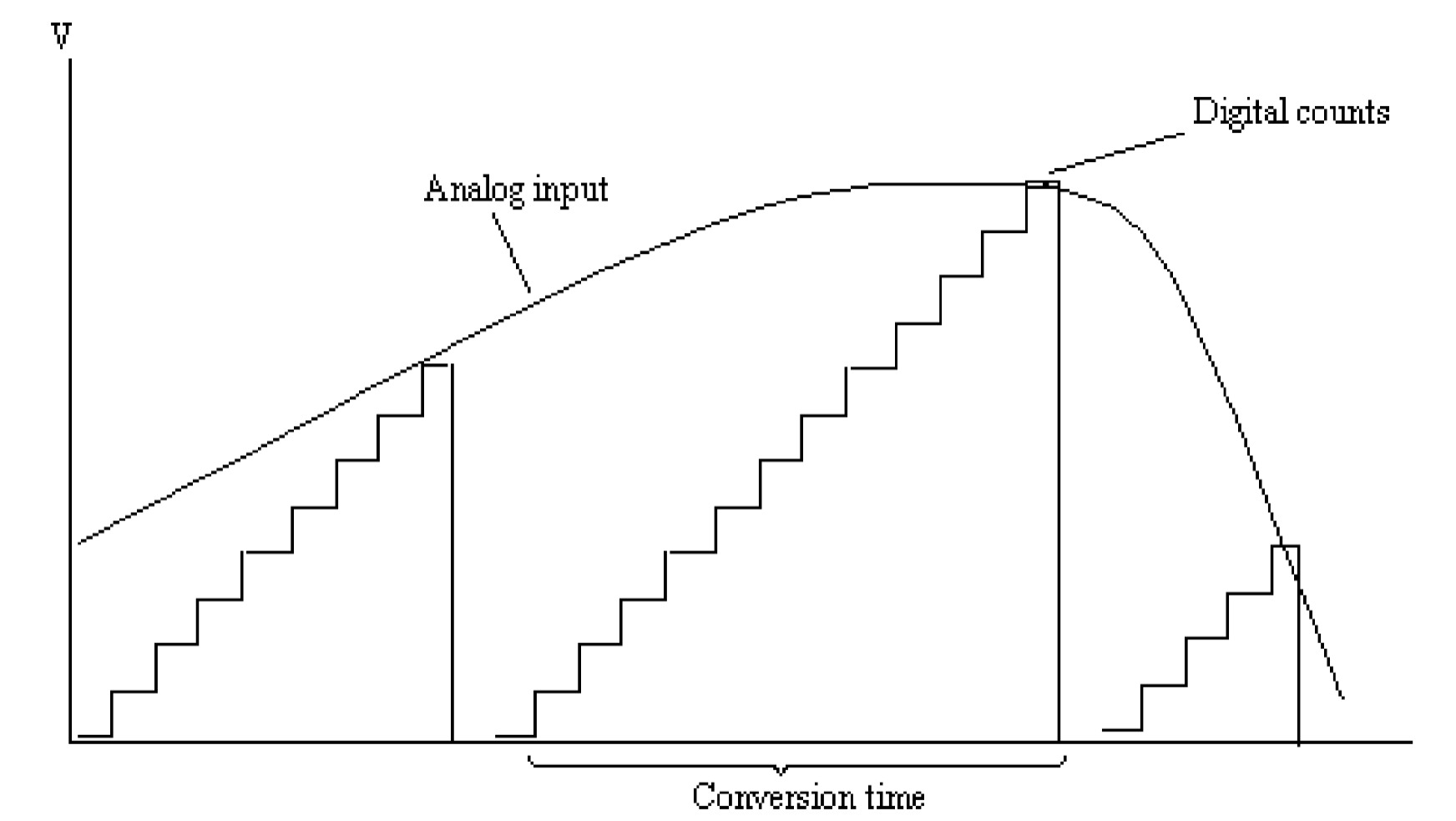
For a steady input, the digital output is shown in the figure. The output is represented by the number of clock pulses counted by the counter until the staircase voltage equals the input voltage. This conversion method is slow; as for maximum input, the counter has to count from zero to a maximum number of states for the comparison. The counter is to be reset for each conversion cycle, and counting starts from the beginning. The conversion time is not important in d.c. or slow varying signals as the output waveform gives a good representation from which the input waveform can be constructed, as shown in the figure. However, if the conversion and signal transient times are comparable, the reconstructed digital output will not be correct. In this case, it is necessary to reduce the conversion time by using a faster D/A converter.
A modification to this converter is possible if the resetting of the counter is avoided each time. For this purpose, an up/down counter may be used instead of an up counter. The circuit shown in the figure illustrates this modification in which an (earlier figure) up/down binary counter is used, and the converter proceeds without resetting. The circuit is almost the same as the counter or digital ramp-type A/D converter. The up/Down counter is operated by up or down signals from the control unit. The digital-to-analog converter output controls the output of the comparator. Till the D/A converter output is less than the analog input voltage, the up signal is enabled, and the counter counts in the forward direction. When the analog input falls, the down signal is enabled, and the counter starts reverse counting, giving an output corresponding to the new analog input, as shown in the figure.
Single Slope A/D converter
This type of method is similar to a counter or digital ramp-type A/D converter. In this type of A/D converter, a gate whose period is proportional to the amplitude of the analog sample is generated. For the generation of the gate, the input analog voltage is compared with the output of an integrator. The output of the integrator is a ramp voltage of constant slope. The standard clock pulses are passed through the gate and are counted by the counter. The gate remains open for the time proportional to the input analog signal. Therefore, the recorded number of pulses is the required digital output of the analog signal.
The schematic block diagram of such an analog-to-digital converter is shown in the figure. A reset pulse is initially applied, which clears the counter and resets the integrator. The integrator produces a linearly rising ramp voltage, whose slope will depend on the resistance \(R\) and capacitor \(C\) values. A comparator compares the input analog voltage with the ramp voltage. The comparator output is high as long as the integrator output is smaller than the input analog voltage. This high output enables the \(AND\) gate. Therefore, the standard clock pulses are allowed to pass through the gate, which will be counted by the counter. When the ramp voltage becomes greater than the input analog voltage, the comparator changes the state, thereby disabling the \(AND\) gate. The counter stops counting. It can easily be seen that the gate duration is linearly related to the magnitude of the input analog signal. Hence, the count accumulated in the counter is a digital representation of the input analog voltage.
Dual Slope A/D converter
In a single slope A/D converter, the accuracy of the converter depends on the linearity of the ramp voltage generated by the integrator. However, the linearity of ramp voltage depends on the accuracy of the values of Resistance \(R\) and capacitance \(C\) of the integrator, whose values may vary with time and temperature. The dual-slope analog-to-digital converter utilizes two different ramps, one for a fixed time and the other for a fixed slope. It is a very popular and widely used D/A converter because it has the slowest conversion time and relatively low cost. This method offers good accuracy, linearity, and noise rejection characteristics.
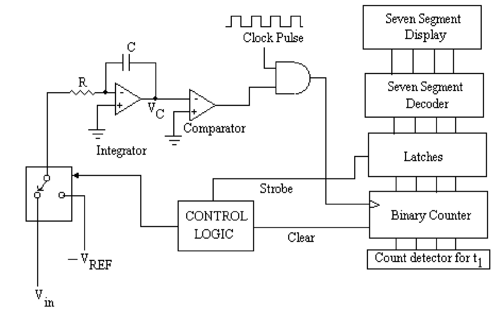
The logic diagram of the dual-slope A/D converter is given in the figure. This converter is similar to that of the single slope A/D converter. In this converter, the integrator forms two different ramps, one for fixed time and the other for fixed slope. The capacitor of the integrator is first charged with constant current obtained from input analog voltage for a fixed time; then, the capacitor is discharged for a fixed slope through other constant current obtained from a reference voltage source. The essential operation of this converter can be understood as follows: This converter consists of standard clock pulses applied to the gate. The gate allows the pulses to input the counter, which counts these pulses. Initially, all the counters are reset to \(0\)’s, and the ramp is reset to zero. Now, the control logic allows switch \(S\) to connect the input analog voltage \(V_{in}\) to the integrator circuit. A constant current equal to \(\frac{V_{in}}{R}\) flows through the capacitor \(C\) as the inverting input of the operational amplifier of the integrator is at virtual ground. The capacitor \(C\) will charge linearly with this constant current. This results in a negative going ramp at the output of the integrator. The comparator's output will be positive, allowing the clock pulse to pass through the \(AND\) gate to the input of the counter. This ramp is allowed for a fixed time, say \(t_1\). The count detector determines the actual time \(t_1\). The voltage \(V_C\) at the output of the integrator is given by:
\[ V_{C}=-\frac{1}{RC}\int_{0}^{t_1}V_{in}~dt = -\frac{1}{RC}V_{in}~t_{1} \]The counter reaches the fixed count at \(t_1\), the control logic generates a pulse to clear the counter to zero, and the switch \(S\) connects the integrator input to a negative reference voltage (\(-V_{REF}\)). The capacitor \(C\) of the integrator starts discharging linearly due to the constant current from \(V_{REF}\). The integrator thus produces a positive going ramp at \(-V_{C}\) and increases steadily until it reaches \(0\) volt, as shown in the figure. At this time, the counter is counting. The conversion cycle ends when \(V_C\) = \(0\) volt; The comparator produces the low state, disables the gate, and the counter stops counting.
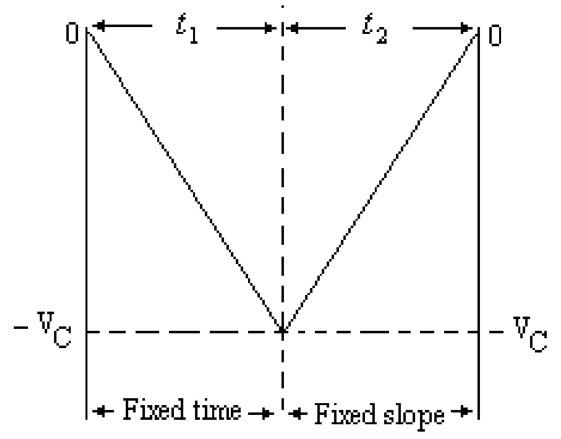
Let \(t_{2}\) be the time when the output of the integrator becomes zero, so the output of the integrator is given by:
\[ V_{C}=-\frac{V_{REF}}{RC}t_{2} \]Since the integrator's output begins at \(0\) volts integrates down to \(-V_{C}\), and then integrates back to \(0\) volts, the equations may be equated as:
\[ -\frac{1}{RC}V_{in}~t_{1}=-\frac{V_{REF}}{RC}~t_{2} \] \[ V_{in}=V_{REF}\frac{t_{2}}{t_{1}} \]In this equation, \(V_{REF}\) and time \(t_1\) are constants, so
\[ V_{in}\propto t_{2} \]This equation is independent of the values of resistance \(R\) and capacitance \(C\). Further, at the end of the conversion cycle, the counts measured by the counter are proportional to the input analog signal and are latched to display devices.