Introduction
Sometimes, the information available for processing is in digital form, while in most cases, it is available in analog form. For example, the outputs of digital voltmeters, digital frequency meters, digital clocks and calculators, etc., are available in digital form. Still, most physical quantities, such as temperature, pressure, light, voltage and current, etc. give information in analog form. It is often necessary to convert information in one form to another form. For example, to convert the temperature (reading of mercury thermometer which is in analog form) in digital readout or in digital form, a transducer such as thermocouple or thermister is first used to convert the physical quantity to electrical quantity; an analog to digital converter then converts this quantity to digital form. Similarly, for plotting the output of a digital system on a curve plotter or X-Y recorder, the digital output is first converted to analog output with the help of digital to analog converter, the output of which drives a servomotor. So analog to digital (A/D) converters or digital to analog (D/A) converters are the interfacing devices that couple the digital system to analog or vice-versa. Here, various types of A/D and D/A converters are discussed.
Digital to Analog converters
Digital to Analog (D/A) converter converts the digital information into analog form. The input may be n-bit long, having different voltage levels. So, in the D/A converters, some method is to be used that can convert this voltage level of n-bits to its equivalent analog form. This can be accomplished by using different resistive networks. The following two types of resistive networks are used for this purpose:
- Resistive Divider Network or weighted resistor network
- Binary Ladder Network or R-2R network
The converter, which comprises the resistive divider network, is known as The resistive divider D/A converter and the D/A converter, which comprises the binary ladder network, is known as the binary ladder D/A converter. These converters will now be discussed separately.
Resistive Divider D/A converter
As discussed above, the resistive divider D/A converter consists of a resistive divider network. So, before discussing the complete circuit diagram of a resistive divider D/A converter, it is better to understand the workings of a resistive divider network. The resistive divider network changes each n-bit digital level into its equivalent analog output. The discussion is now about converting the n-bit digital input to its equivalent analog signal. A weight is assigned to each bit of n-bit digital input, so the weighted sum must equal 1. In general, the binary weight assigned to LSB in an n-bit digital input is \(\frac{1}{2^n-1}\). The weights assigned to \(2^{nd}\) LSB, \(3^{rd}\) LSB, \(4^{th}\) LSB, and so on are obtained by multiplying the weight of LSB to \(2^1=2\), \(2^2=4\), \(2^3=8\), etc. respectively. For instance, weights assigned to different bits of 4-bit binary input \(b_3\) \(b_2\) \(b_1\) \(b_0\) are:
- Weight assigned to LSB \(b_0\) bit is \(\frac{2^0}{2^4-1}=\frac{1}{15}\)
- Weight assigned to 2nd LSB \(b_1\) bit is \(\frac{2^1}{2^4-1}=\frac{2}{15}\)
- Weight assigned to 3rd LSB \(b_2\) bit is \(\frac{2^2}{2^4-1}=\frac{4}{15}\)
- Weight assigned to MSB \(b_3\) bit is \(\frac{2^3}{2^4-1}=\frac{8}{15}\)
- The sum of weights assigned to each bit of 4-bit digital input is 1 as \(\frac{1}{15}+\frac{2}{15}+\frac{4}{15}+\frac{8}{15}=1\).
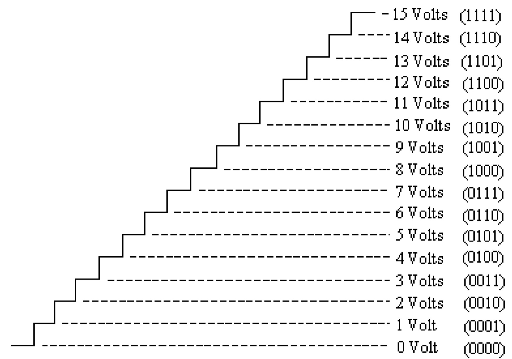
In a four-bit binary system, there will be 16 different possible input combinations, corresponding to which the analog signal will be obtained if it is assumed that a certain reference voltage \(V_{REF}\) is applied whenever there is a 1 in a binary bit. In a 4-bit digital system, if \(V_{REF}\) =15 volts, the analog voltage available for each combination of binary input should be as given in the table.
| \(b_{3}\) | \(b_{2}\) | \(b_{1}\) | \(b_{0}\) | Weight | Analog Voltage |
|---|---|---|---|---|---|
| 0 | 0 | 0 | 0 | 0/15 | \((0/15)V_{REF}=0\) volt |
| 0 | 0 | 0 | 1 | 1/15 | \((1/15)V_{REF}=1\) volt |
| 0 | 0 | 1 | 0 | 2/15 | \((2/15)V_{REF}=2\) volt |
| 0 | 0 | 1 | 1 | 3/15 | \((3/15)V_{REF}=3\) volt |
| 0 | 1 | 0 | 0 | 4/15 | \((4/15)V_{REF}=4\) volt |
| 0 | 1 | 0 | 1 | 5/15 | \((5/15)V_{REF}=5\) volt |
| 0 | 1 | 1 | 0 | 6/15 | \((6/15)V_{REF}=6\) volt |
| 0 | 1 | 1 | 1 | 7/15 | \((7/15)V_{REF}=7\) volt |
| 1 | 0 | 0 | 0 | 8/15 | \((8/15)V_{REF}=8\) volt |
| 1 | 0 | 0 | 1 | 9/15 | \((9/15)V_{REF}=9\) volt |
| 1 | 0 | 1 | 0 | 10/15 | \((10/15)V_{REF}=10\) volt |
| 1 | 0 | 1 | 1 | 11/15 | \((11/15)V_{REF}=11\) volt |
| 1 | 1 | 0 | 0 | 12/15 | \((12/15)V_{REF}=12\) volt |
| 1 | 1 | 0 | 1 | 13/15 | \((13/15)V_{REF}=13\) volt |
| 1 | 1 | 1 | 0 | 14/15 | \((14/15)V_{REF}=14\) volt |
| 1 | 1 | 1 | 1 | 15/15 | \((15/15)V_{REF}=15\) volt |
So the analog voltage for binary word = (weight of the binary word) \( \times V_{REF}\)
It may be noted from table that the analog voltage corresponding to the binary equivalent is a discrete step value, as given in the figure. The discrete step is of 1 volt if \(V_{REF}\) is assumed to be 15 volts in a four-bit digital input. The step voltage (analog) will be dependent on the reference voltage. There will, however, be \(2^n\) steps in the \(n\)-bit digital system.
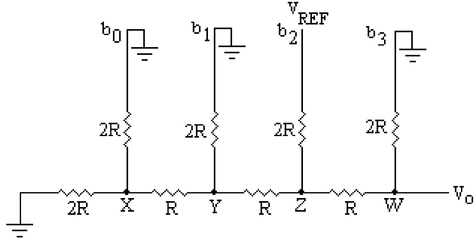
Resistive divider network is used for converting digital inputs to analog outputs. The network for 6 bit binary system shown in figure is known as the weighted network, as the resistors are weighted inversely with their current values. The input binary bits are \(b_5\), \(b_4\), \(b_3\), \(b_2\), \(b_1\), \(b_0\) where \(b_0\) is the LSB and \(b_5\) is MSB. These binary bits may be logic 0 or 1. Logic 0 may further be assumed as 0 volt and logic 1 as \(V_{REF}\). So \(V_0\), \(V_1\), \(V_2\), \(V_3\), \(V_4\) and \(V_5\) are the input voltage levels which may be 0 volt or \(V_{REF}\) depending on the binary bits. The resistors \(R_0\), \(R_1\), \(R_2\), \(R_3\), \(R_4\) and \(R_5\) are connected to bits \(b_0\), \(b_1\), \(b_2\), \(b_3\), \(b_4\), \(b_5\) respectively. It may be noted from this network that the resistor connected to the binary bit is half the value of resistor connected to the previous (lower bit). Hence this network also called as the resistive divider network. Let \(R_L\) is the load resistance which is supposed to very high i.e. very much higher than the resistor \(R_0\).
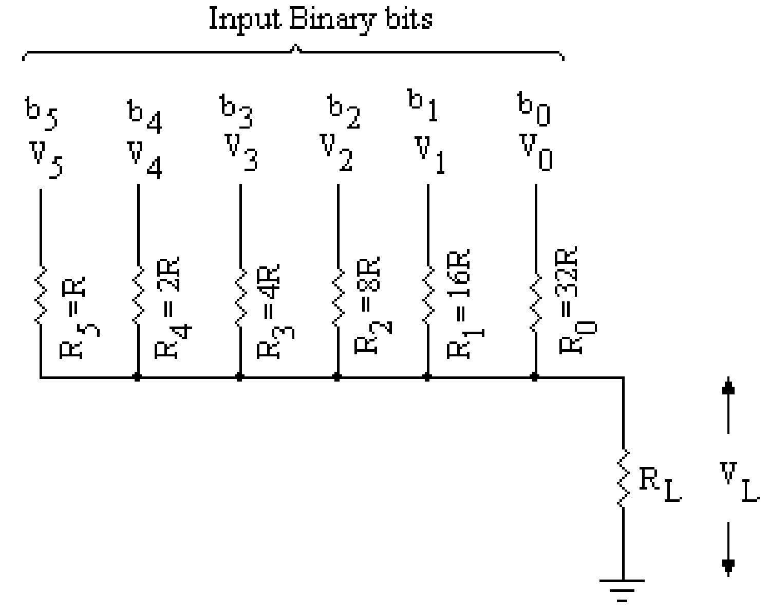
Now the voltage \(V_L\) across the load resistance \(R_L\) can be obtained by Ohm's law.
\[V_L=I_{eff} \times R_{eff}\] \[ V_L=\frac{I_{eff}}{\left(\frac{1}{R_{eff}}\right)} \] \[ V_L=\frac{I_{5}+I_{4}+I_{3}+I_{2}+I_{1}+I_{0}}{\left(\frac{1}{R_{eff}}\right)} \] \[ V_L=\frac{\left(\frac{V_{5}}{R_{5}}+\frac{V_{4}}{R_{4}}+\frac{V_{3}}{R_{3}}+\frac{V_{2}}{R_{2}}+\frac{V_{1}}{R_{1}}+\frac{V_{0}}{R_{0}}\right)}{\left(\frac{1}{R_{5}}+\frac{1}{R_{4}}+\frac{1}{R_{3}}+\frac{1}{R_{2}}+\frac{1}{R_{1}}+\frac{1}{R_{0}}\right)} \] \[ V_L=\frac{\left(\frac{V_{5}}{R}+\frac{V_{4}}{2R}+\frac{V_{3}}{4R}+\frac{V_{2}}{8R}+\frac{V_{1}}{16R}+\frac{V_{0}}{32R}\right)}{\left(\frac{1}{R}+\frac{1}{2R}+\frac{1}{4R}+\frac{1}{8R}+\frac{1}{16R}+\frac{1}{32R}\right)} \] \[ V_L=\frac{(V_{5}+V_{4}+V_{3}+V_{2}+V_{1}+V_{0})}{(32+16+8+4+2+1)} \] \[ V_L=\frac{(V_{5}+V_{4}+V_{3}+V_{2}+V_{1}+V_{0})}{63} \] \[ V_L=\frac{1}{(2^6-1)}(2^{5}V_{5}+2^{4}V_{4}+2^{3}V_{3}+2^{2}V_{2}+2^{1}V_{1}+2^{0}V_{0}) \] \[ V_L=\frac{1}{(2^6-1)}\left([2^{5}b_{5} V_{REF}]+[2^{4}b_{4} V_{REF}]+[2^{3}b_{3} V_{REF}]+[2^{2}b_{2} V_{REF}]+[2^{1}b_{1} V_{REF}]+[2^{0}b_{0} V_{REF}]\right) \] \[ V_L=\frac{V_{REF}}{(2^6-1)}(2^{5}b_{5}+2^{4}b_{4}+2^{3}b_{3}+2^{2}b_{2}+2^{1}b_{1}+2^{0}b_{0}) \]From this equation, it is clear that if the input binary bits are all 1 (in a six-bit system) and the reference voltage (V_REF) = 6.4 volts (say), the \(V_L\) is given by:
\[ V_L=\frac{V_{REF}}{63} \times 63 = 6.4~volts \]The output of this network is as per our requirement and is proportional to the input binary data. In general, the equation for the output voltage of \(n\)-bit binary digits is given as:
\[ V_L=\frac{V_{REF}}{(2^n-1)}(2^{n-1}b_{n-1}+\dots+2^{4}b_{4}+2^{3}b_{3}+2^{2}b_{2}+2^{1}b_{1}+2^{0}b_{0}) \]
Example 1: A 6-bit resistive divider network has 10 volts full-scale output, find output voltage for an input of 110110.
Solution:
Given:
- \(V_{REF}=10 volts\) and Binary input: 110110
- \(b_5=1,b_4=1,b_3=0,b_2=1,b_1=1,b_0=0\)
The output voltage for 6 bit resistive divider network is given by:
\[ V_L=\frac{V_{REF}}{(2^6-1)}(2^{5} \times b_{5}+2^{4} \times b_{4}+2^{3} \times b_{3}+2^{2} \times b_{2}+2^{1} \times b_{1}+2^{0} \times b_{0}) \] \[ V_L=\frac{10}{(2^6-1)}(2^{5} \times 1+2^{4} \times 1+2^{3} \times 0+2^{2} \times 1+2^{1} \times 1+2^{0} \times 0) \] \[ V_L=\frac{10}{63}(32+16+0+4+2+0) = \frac{540}{63} = 8.57~volts \]Binary Ladder D/A Converter
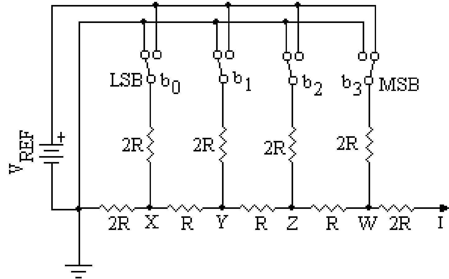
A more commonly used D/A converter is a binary ladder D/A converter, which removes the drawbacks in the resistive divider D/A converter. This type of D/A converter contains an \(R-2R\) ladder network. The \(R-2R\) resistive ladder network gives the output a weighted sum of digital inputs. Such a ladder network for 4-bit input is shown in the figure. This network has only two resistor values, i.e., \(R\) and \(2R\). In this network, \(b_0\), \(b_1\), \(b_2\), and \(b_3\) are the input binary bits and \(b_0\) is the LSB and MSB is \(b_3\). Any of these bits will be at the ground potential when the corresponding bit is at logic \(0\) or the reference potential \(V_{REF}\) when the input bit is at logic \(1\).
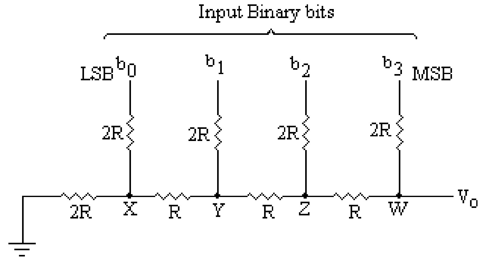
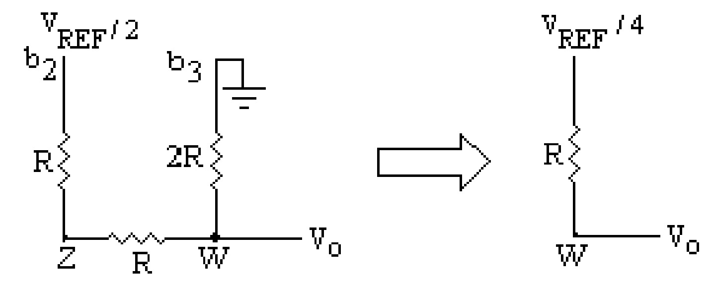
To examine the behavior of this network, it is assumed that the bit \(b_3\) is at logic \(1\) (or \(V_{REF}\) potential) as shown in figure.
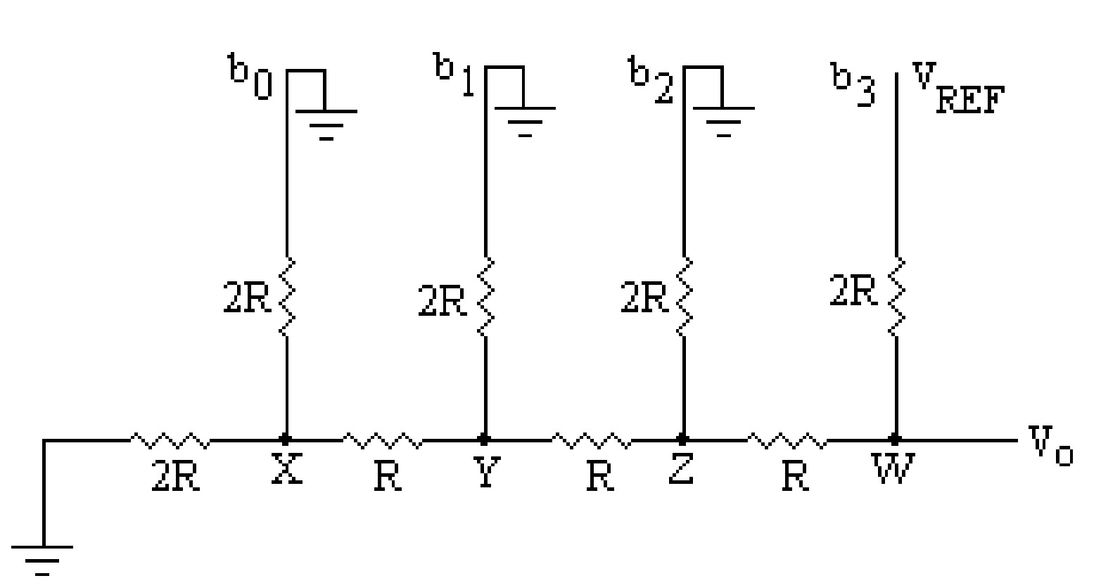
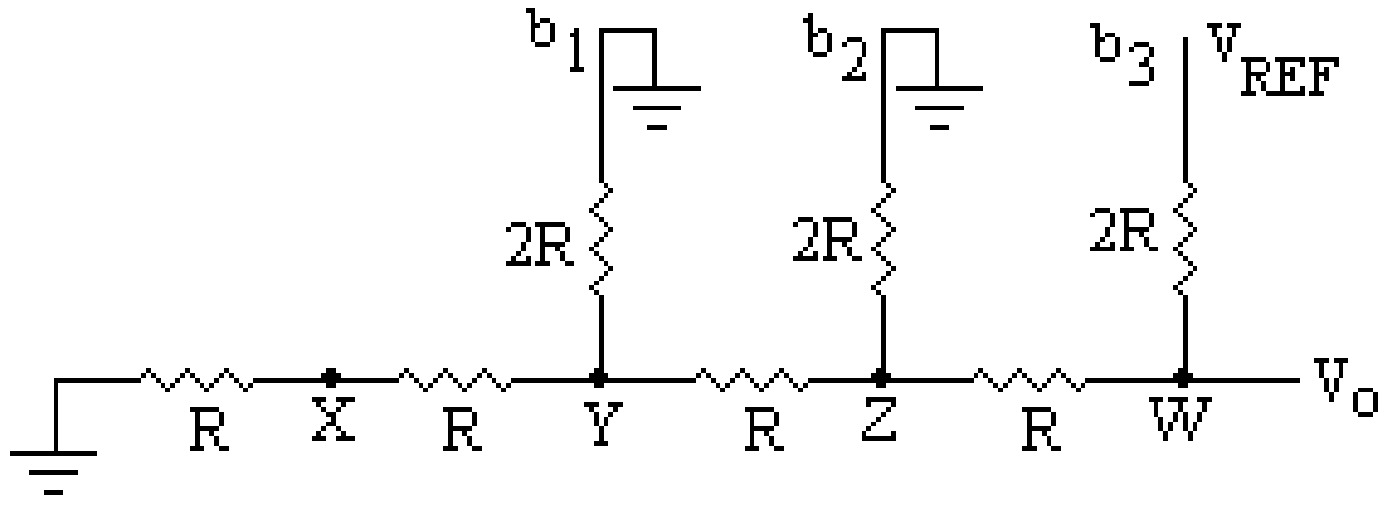
From figure, it is clear that the resistance at point (W) and ground is \(2R\), and the resistance towards bit \(b_3\) is also \(2R\). Thus, the output voltage at the point \(W\) due to bit \(b_3\) (MSB) assumed at \(V_{REF}\) potential is given by:
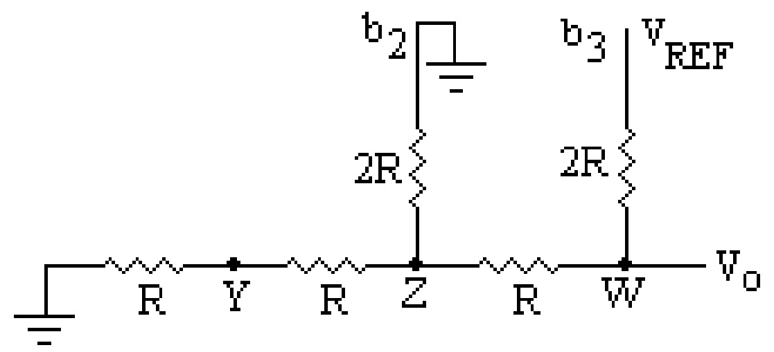
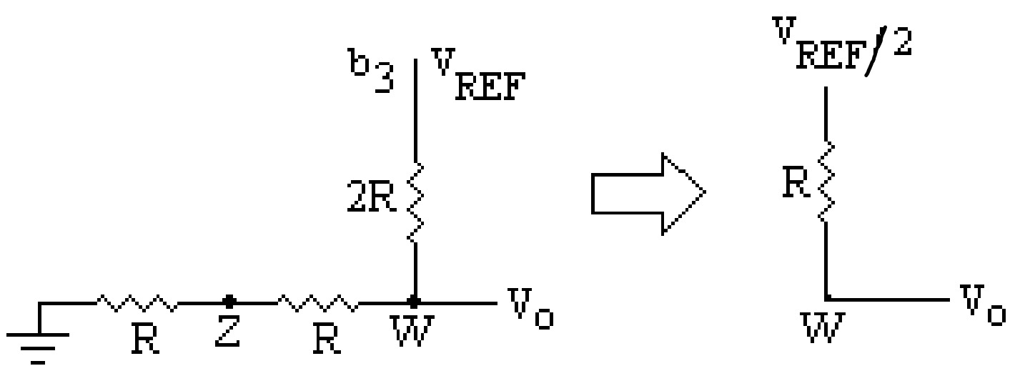
The output voltage \(V_0\) due to the binary input 1000 (only MSB is high) is half of the reference voltage with effective resistance \(R\) in series. Similarly, one can calculate the output voltage due to the binary input 0100 (i.e., second MSB). the output voltage due to the second MSB (or for binary input 0100) is \(\frac{V_{REF}}{4}\) with effective resistance \(R\) in series with it.
It can further be shown that the output due to third MSB (for binary input 0010) is \(\frac{V_{REF}}{8}\). And for LSB (0001 binary input) the output is \(\frac{V_{REF}}{16}\). Each voltage source will have effective resistance \(R\) in series with the source. The total output voltage in analog form, due to all the inputs as \(1\) (for \(1111\)) can easily be found by adding the outputs obtained for each bit as given below:
\[ V_0=\frac{V_{REF}}{2}+\frac{V_{REF}}{4}+\frac{V_{REF}}{8}+\frac{V_{REF}}{16} \] \[ V_0=\frac{V_{REF}}{16}\left(8\times b_{3}+4\times b_{2}+2\times b_{1}+1\times b_{0}\right) \] \[ V_0=\frac{V_{REF}}{2^{4}}\left(2^{3}\times b_{3}+2^{2}\times b_{2}+2^{1}\times b_{1}+2^{0}\times b_{0}\right) \]This equation represents the voltage at the output of 4 bit binary ladder network. A general equation for the output of \(n\)-bit binary data can be given as follows:
\[ V_0=\frac{V_{REF}}{2^{n}}\left(2^{n-1}\times b_{n-1}+\dots+2^{3}\times b_{3}+2^{2}\times b_{2}+2^{1}\times b_{1}+2^{0}\times b_{0}\right) \]The output of this network is proportional to the input binary data. So using this \(R-2R\) ladder network, a D/A converter (called binary ladder D/A converter) can be designed.
Example 2: For a five-bit binary ladder D/A converter the input levels are \(0\) = \(0\) volt and \(1\) = \(+ 10\) volts, find
- (i) the output voltages caused by each bit
- (ii) the output voltage corresponding to an input of \(10110\)
- (iii) the full-scale output voltage of the ladder.
Solution:
(i)
- The output voltage caused by MSB =\(\frac{V_{REF}}{2}\)=\(\frac{10}{2}\) = \(5\) volts
- The output voltage caused by MSB =\(\frac{V_{REF}}{4}\)=\(\frac{10}{4}\) = \(2.5\) volts
- The output voltage caused by MSB =\(\frac{V_{REF}}{8}\)=\(\frac{10}{8}\) = \(1.25\) volts
- The output voltage caused by MSB =\(\frac{V_{REF}}{16}\)=\(\frac{10}{16}\) = \(0.625\) volts
- The output voltage caused by LSB =\(\frac{V_{REF}}{32}\)=\(\frac{10}{32}\) = \(0.3125\) volts
(ii)
The output voltage corresponding to an input of \(10110\) is
\[ V_0=\frac{V_{REF}}{2^{5}}\left(2^{4}\times b_{4}+2^{3}\times b_{3}+2^{2}\times b_{2}+2^{1}\times b_{1}+2^{0}\times b_{0}\right) \] \[ V_0=\frac{10}{32}\left(2^{4}\times 1+2^{3}\times 0+2^{2}\times 1+2^{1}\times 1+2^{0}\times 0\right) \] \[ V_0=\frac{10}{32}\left(16+0+4+2+0\right) \] \[ V_0=\frac{220}{32}=6.875~ volts \](iii)
The full-scale output voltage is given by:
\[ V_0=\frac{V_{REF}}{2^{5}}\left(2^{4}\times b_{4}+\dots+2^{3}\times b_{3}+2^{2}\times b_{2}+2^{1}\times b_{1}+2^{0}\times b_{0}\right) \] \[ V_0=\frac{10}{32}\left(2^{4}\times 1+2^{3}\times 1+2^{2}\times 1+2^{1}\times 1+2^{0}\times 1\right) \] \[ V_0=\frac{10}{32}\left(16+8+4+2+1\right) \] \[ V_0=\frac{310}{32}=9.6875~volts \]Performance criteria for D/A converters
The D/A converters are available in ICs with different specifications for their performances. The important characteristics of the D/A converters are given below:
- Resolution
- Accuracy
- Monotonicity
- Settling time
Resolution
The analog output of the D/A converter is proportional to the digital input (binary data), so a perfect staircase is obtained if there is an LSB increment. The resolution is, therefore, a measure of the quality of the D/A converter, defined as the ratio of the LSB increment to the maximum output. For an \(n\)-bit D/A converter, the resolution is given by: The change in output due to LSB increment for \(n\)-bit digital input (Step size) \[ Resolution = \frac{Full~scale~output}{No.~ of~ steps} = \frac{Full ~scale~ output}{(2^n−1)} \]
where \((2^n−1)\) is the number of steps for \(n\)-bit D/A converter.
\[ Percentage~Resolution =\frac{Full ~scale ~output/(2^n−1)}{Full~ scale ~output} \times 100 \] \[ \frac{1}{(2^n−1)} \times 100 \]The step size for a \(10\)-bit D/A converter, having a full-scale output voltage of \(10\) volts is given by
and Percentage Resolution \(=0.0978~\%\) percent
Accuracy
The accuracy of a D/A converter is the closeness of the output analog voltage to the expected theoretical output. In a linear variation of analog output with digital input, the relative accuracy is the maximum deviation of the D/A output compared with the linear behavior. It is expressed as a percent of a full-scale or maximum output voltage. For example, if a converter has a full-scale output of 10 V and the accuracy is \(\pm~1.0~\% \), then the maximum error for any output voltage is (10V)(0.001) = 10 mV. Ideally, the accuracy should be at most \(\pm~\frac{1}{2} \) of an LSB. For an 8-bit D/A converter, one LSB is \(\frac{1}{256} = 0.0039 = 0.39 ~\%\) of full scale. The accuracy should be approximately \(\pm 0.2 ~\%\).
Monotonicity
A D/A converter is said to be monotonic if it gives an analog output voltage increases regularly and linearly with an increase in input digital signal. Such a quality of the converter is called monotonicity. To demonstrate the monotonicity of a D/A converter, a counter output is given as digital input to a D/A converter, and the analog output is displayed on the CRO. Monotonicity then requires that the output waveform should be a perfect staircase waveform with steps equally spaced and of the same amplitude. If the steps are missing or have varying amplitude, the D/A converter is defective.
Settling time
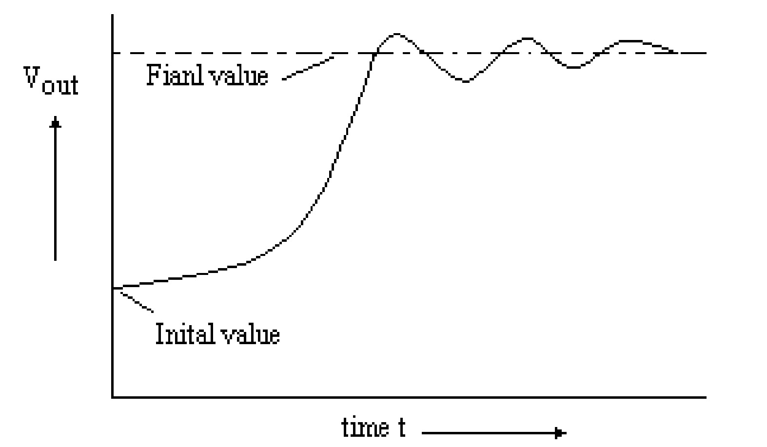
After applying digital input to a D/A converter, it takes a few nanoseconds to microseconds to produce the correct output. So, the settling time is defined as the time the converter takes to give an output to settle within \(\pm \frac{1}{2}\) LSB of its final value. For example, if a D/A converter has a resolution of \(10\) mV, the settling time measures the time the converter takes to settle within \(\pm\) \(5\) mV of its final value. Figure illustrates the settling time in a D/A converter. The settling time is crucial because it limits how fast one can change the digital input. The settling time depends on the stray capacitance, saturation delay time, and other factors.
Example 3: What is the step size (or resolution in volts) of a 12 bit D/A converter, if the full scale output is +10 volts? Find the percentage resolution also.
Solution:
- Given: \(n = 12\)
- Step size is given by
Example 4: How many bits are required at the input of a D/A converter to achieve a resolution of 10mV, if the full scale output is 10 volts?
Solution:
- Given: Resolution: (10) mV
\[ Resolution = \frac{Full~scale~output}{2^n-1} \]
\[ 10~mV = \frac{10}{2^{n}-1} \]
\[ 2^{n}-1 = \frac{10}{10 \times 10^{-3}} =1000 \]
\[ 2^{n} = 1001 \sim 2^{10} \]
\[ n=10 \] So the number of bits required = \(10\)