Multiplexers:
A multiplexer (MUX) also known as data selector, is a logic circuit which allows the digital information from multi-inputs to a single output line. The selection of the input data to be routed to the output line is done by the select terminals. The number of select terminals depends on the number of input lines to be routed to output line, given by the general formula as:
\[ 2^K = N \]where (N) is the number of input lines and (K) is the number of select terminals. In other words, if there are 4 input lines to be routed to output line, then two select terminals are needed as \(2^2=4\).
The block diagram for 4:1 multiplexer is shown in figure.

In which \(X_0\), \(X_1\), \(X_2\), \(X_3\), are the 4 input lines and \(S_1\), \(S_0\) are the select terminals and \(X\) is the output terminal. Normally a strobe terminal or enable terminal \(G\) is provided in the MUXs which is normally active-low. The active-low means it performs the operation when it is low; it also helps to cascade the MUXs. The Boolean function to perform the multiplexing action is given as:
\[X = X_0~\overline{S_1}~\overline{S_0} + X_1~\overline{S_1}~S_0 + X_2~S_1~ \overline{S_0} + X_2~ S_1~ S_0\]The output \(X\) will follow the input data depending on the select terminals \(S_1\), \(S_0\) as given in the table
| Select terminals | Output | |
|---|---|---|
| \(S_1\) | \(S_0\) | \(X\) |
| \(0\) | \(0\) | \(X = X_0\) |
| \(0\) | \(1\) | \(X = X_1\) |
| \(1\) | \(0\) | \(X = X_2\) |
| \(1\) | \(1\) | \(X = X_3\) |
Note that only one of the inputs \(X_0\), \(X_1\), \(X_2\), \(X_3\) is routed to the output \(X\) (one at a time). The realization of the Boolean function \(X\) with NAND gates only is shown in figure.
The MUXs are available in the form of the following IC's:
IC 74157quadruple two – input multiplexer/data selector.IC 74151Aeight - input multiplexer/data selector.IC 74150sixteen - input multiplexer/data selector.
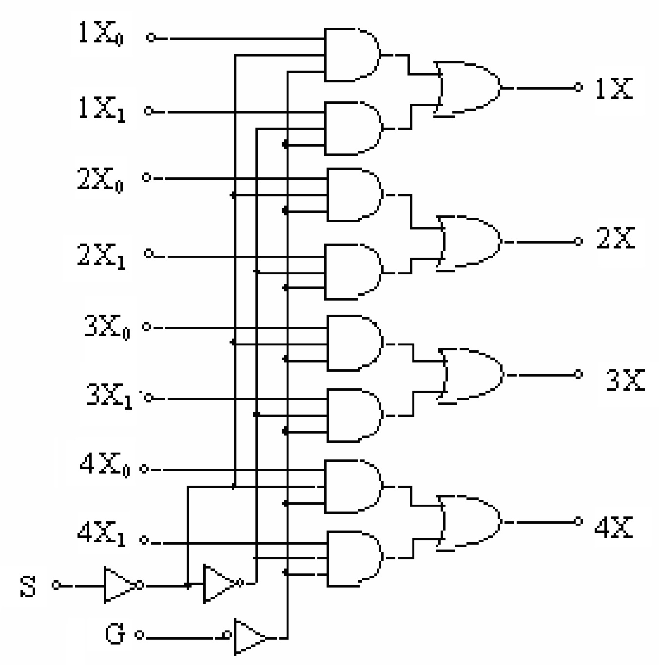
74157 Quadruple two – input multiplexer/data selector:
The internal logic diagram of the IC 74157 is given in figure. It consists of four two input multiplexers on a single chip. Each of the four multiplexers has a common data select line \(S\) and a common chip enable terminal \(G\). A low signal to the chip enable terminal \(G\) allows the selected input data to rout to the output. Since there are only two inputs to be selected from each multiplexer, a single data select terminal is sufficient.
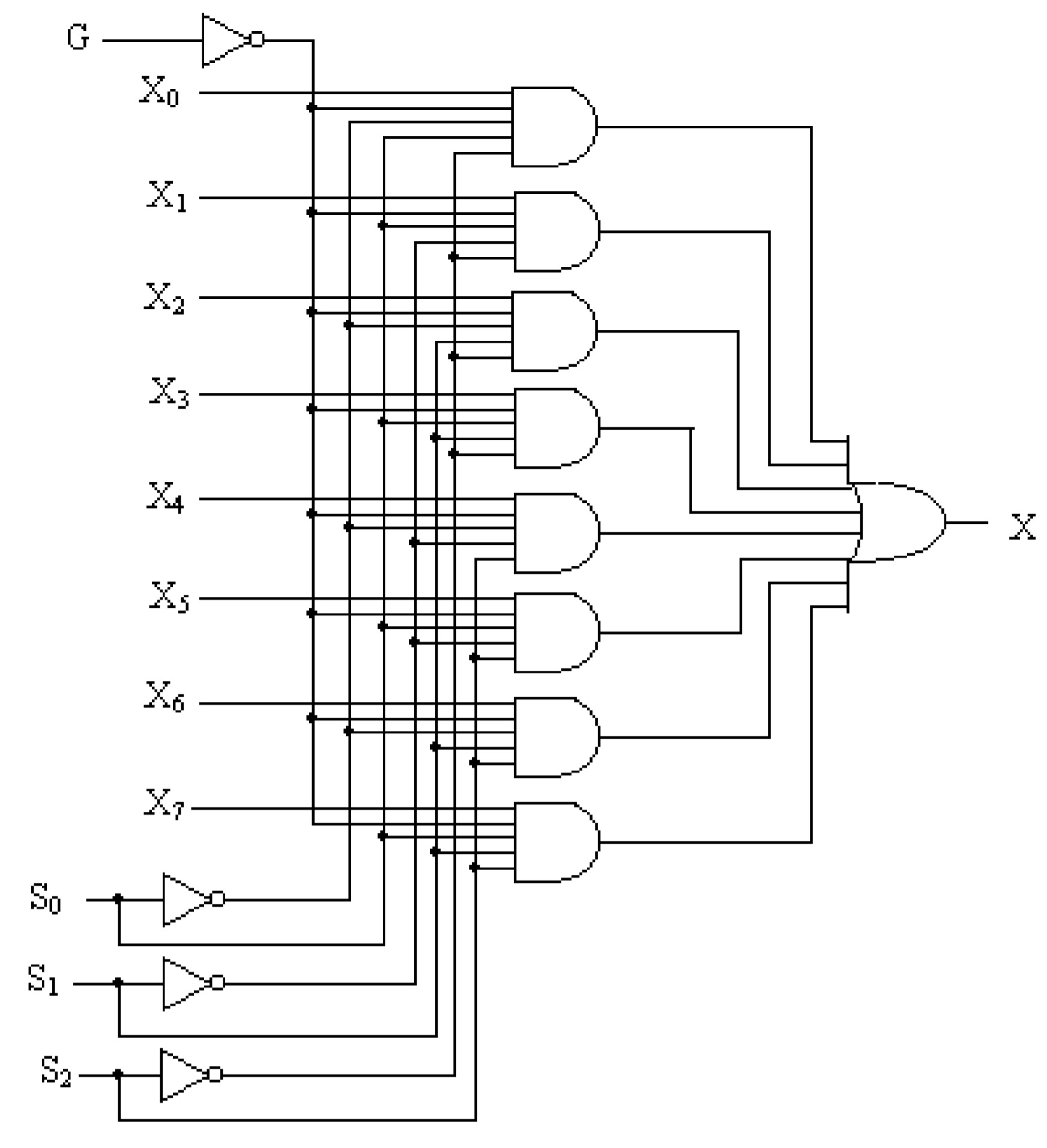
74151A Eight - input multiplexer/data selector:
Figure shows the logic block diagram for a 8 – input multiplexer/ data selector IC 74151A. It has 8 data inputs \(X_0\) through \(X_7\), three data select terminals \(S_2\), \(S_1\), & \(S_0\) and an enable terminal \(G\). when enable terminal \(G\) is high, the multiplexer is disabled and output \(X\) is zero irrespective of the select input terminal. However, when the enable terminal \(G\) is low the input data is routed to the output as per data select terminals \(S_2\), \(S_1\), & \(S_0\) as illustrated in table.
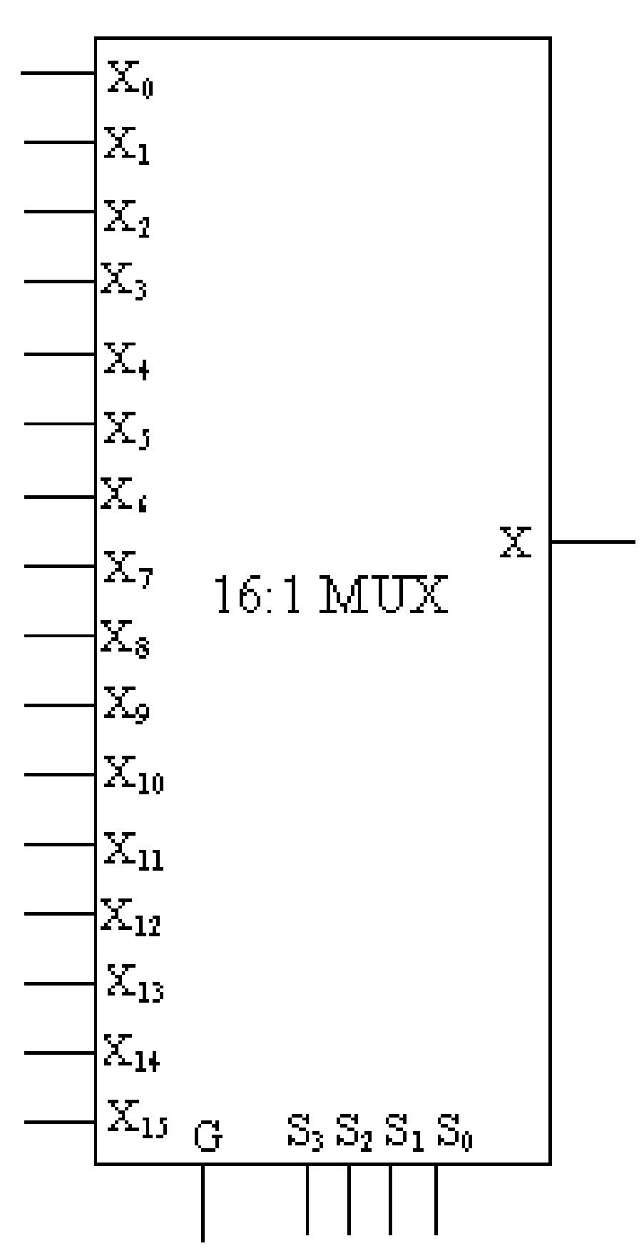
74150 Sixteen - input multiplexer/data selector:
The IC 74150 is 16:1 multiplexer having 16 input lines and one output line. It has four select terminals \(S_3\), \(S_2\), \(S_1\) & \(S_0\) and one enable terminal \(G\) which is kept low for multiplexing action. The block diagram of the 16:1 MUX is given in figure.
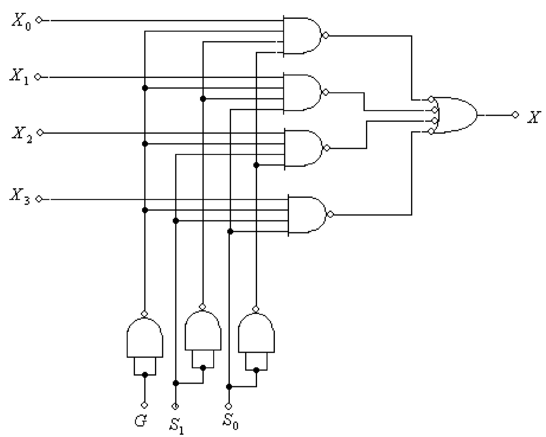
Expansion of Multiplexers:
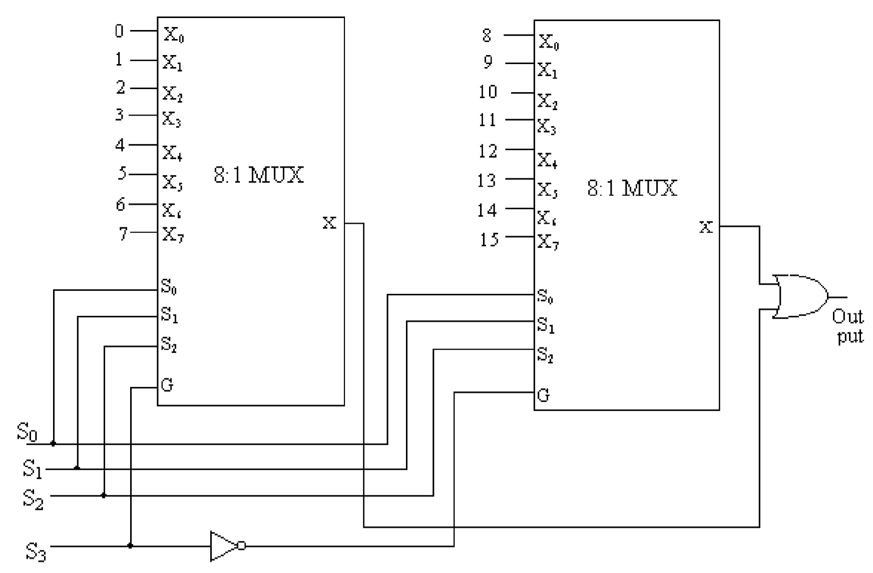
For the expansion of number of input terminals of the multiplexers two MUXs may be cascaded. Two 4:1 MUXs may be cascaded to form 8:1 MUX. Similarly two 8:1 MUXs may be cascaded to have a 16:1 multiplexer and so on. Figure illustrates how two 4:1 MUXs are cascaded to form 8:1 MUX. The enable terminal G of the MUXs in-conjunction with a NOT gate provides the third select terminal. When \(S_2\) is zero the first MUX will be enabled and inputs \(X_0\) through \(X_3\) will be routed to its output; and when \(S_{2}\) is 1, the second MUX will be enabled, \(X_4\) through \(X_7\) will be routed to the output of the second MUX. The outputs of the two MUXs are connected to the inputs of an OR gate which then gives the final output.
Applications of Multiplexers:
Primary aim of the MUXs is the multiplexing operation, that is, the selected input is routed to the output. In addition to this, Implementation of Boolean function can easily be done with MUXs, since MUXs are available in the form of integrated circuits. The method of implementing the Boolean function is that the truth table is first constructed for the given function to be implemented. Then logic \(1\) is connected to each data input of the multiplexer corresponding to each combination of the input variables which has \(1\) in the output column of the truth table. The logic \(0\) is, however, connected to the remaining inputs of the MUX. The variables are connected to the data select inputs of the multiplexer. The Boolean functions of \(N\) – variables can also be implemented by the Multiplexers of \(N – 1\) select lines. A function of 4 variables can be implemented with 8:1 multiplexer having 3 select lines. Let \(A\), \(B\), \(C\), \(D\) are the input variables of the function \(F\), which is to be implemented with a multiplexer. The variable \(A\) is the most significant bit and \(D\) is the least significant bit. Variables \(B\), \(C\), \(D\) are assumed to be the select terminals for the multiplexer. The truth table is drawn for the given function. It is well known that in the truth table variables \(B\)\(C\)\(D\) progresses twice through the sequence \(000\), \(001\), \(\dots\), \(111\); once with \(A = 0\) and other with \(A = 1\). The connections to be made to the data inputs of the multiplexer, following rules are observed.
- A logical \(0\) is connected to the data input of MUX, if the \(0\) occurs at the output in the truth table, both times when MSB is \(0\) and \(1\) (other variables having the same value).
- A logical \(1\) is connected to the data input of MUX, if the \(1\) occurs at the output in the truth table, both times when MSB is \(0\) and \(1\) (other variables having the same value).
- MSB is connected to the data input of MUX, if the output in the truth table is different both times when MSB is \(0\) and \(1\) (other variables having the same value); and also output is the same as the MSB.
- The complement of the MSB is connected to the data input of MUX, if the output in the truth table is same both times when MSB is \(0\) and \(1\) (other variables having the same value); and also output is the same as the complement of MSB.
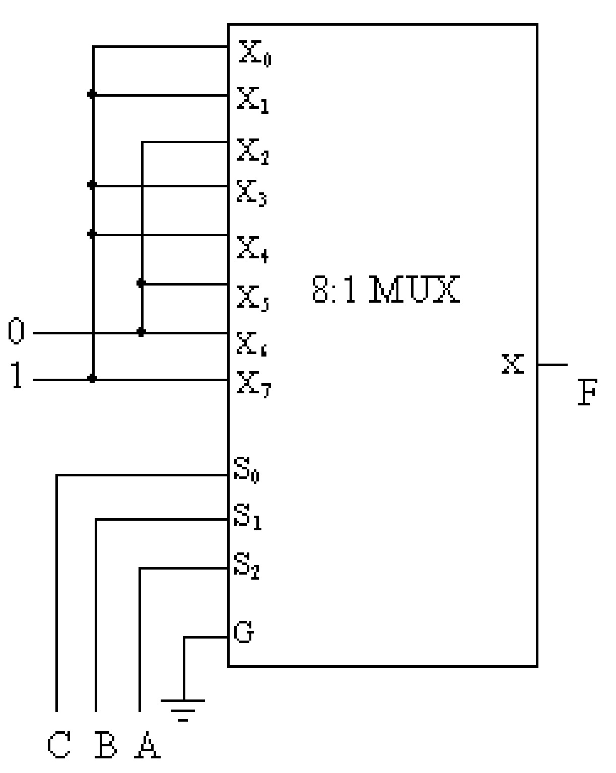
Example 6.1: Realize the following function of three variables with 8:1 MUX. \(F ( A, B, C ) = \Sigma (0, 1, 3, 4, 7)\)
Solution:
The truth table of the given function is drawn as shown in table. To realize the given function using 8:1 MUX, the variable \(A\), \(B\), \(C\) are assumed to be the three select terminals as shown in figure. The logic \(1\) is connected to each data input of the multiplexer corresponding to each combination of the input variables which has \(1\) in the output column of the truth table. The logic \(0\) is connected to the remaining inputs of the MUX. The inputs \(X_0\), \(X_1\), \(X_3\), \(X_4\), X7 are, therefore, connected to the logic \(1\) and \(X_2\), \(X5\), \(X6\) are connected to logic \(0\).
| \(A\) | \(B\) | \(C\) | \(F\) |
|---|---|---|---|
| \(0\) | \(0\) | \(0\) | \(X_0=1\) |
| \(0\) | \(0\) | \(1\) | \(X_1=1\) |
| \(0\) | \(1\) | \(0\) | \(X_2=0\) |
| \(0\) | \(1\) | \(1\) | \(X_3=1\) |
| \(1\) | \(0\) | \(0\) | \(X_4=0\) |
| \(1\) | \(0\) | \(1\) | \(X_5=0\) |
| \(1\) | \(1\) | \(0\) | \(X_6=0\) |
| \(1\) | \(1\) | \(1\) | \(X_7=1\) |
Example 6.2: Use Multiplexers to implement of Full adder.
Solution:
It is well known that a full adder adds three bits of information. Let \(A\), \(B\), \(C\) are three bits to be added. Let augend bit is \(A\), addend bit is \(B\) and \(C\) is the carry from the previous column; \(SUM\) and \(CARRY\) to the next bit are given in the table. Implementation of \(SUM\) and \(CARRY\) is shown in figure.
| A | B | C | SUM MUX | CARRY MUX |
|---|---|---|---|---|
| 0 | 0 | 0 | \(X_0\)=0 | \(X_0\)=0 |
| 0 | 0 | 1 | \(X_1\)=1 | \(X_1\)=0 |
| 0 | 1 | 0 | \(X_2\)=1 | \(X_2\)=0 |
| 0 | 1 | 1 | \(X_3\)=0 | \(X_3\)=1 |
| 1 | 0 | 0 | \(X_4\)=1 | \(X_4\)=0 |
| 1 | 0 | 1 | \(X_5\)=0 | \(X_5\)=1 |
| 1 | 1 | 0 | \(X_6\)=1 | \(X_6\)=0 |
| 1 | 1 | 1 | \(X_7\)=1 | \(X_7\)=1 |

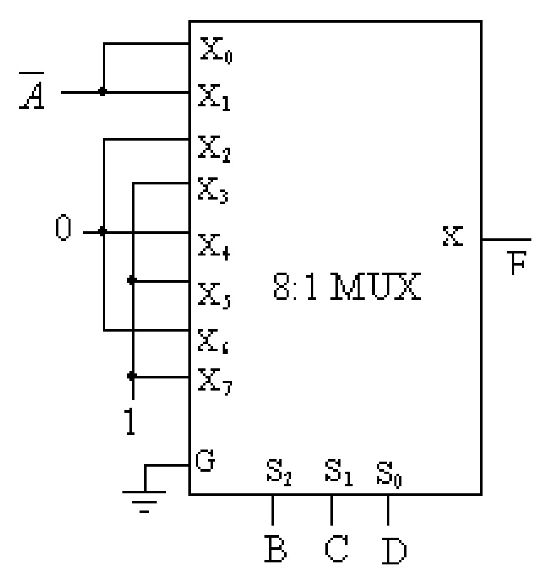
Example 6.3: Realize the following function of four variables with 8:1 MUX.
\[F ( A, B , C , D ) = ∑ (0, 1, 3, 5, 7, 11, 13, 15)\]Solution: The truth table for the given function is first of all drawn (table) and \(Y\), \(Z\), \(W\) are assumed to be the select terminals of the 8:1 MUX. The inputs to the multiplexer are obtained from the truth table as given below.
| A | B | C | D | F | MUX |
|---|---|---|---|---|---|
| 0 | 0 | 0 | 0 | 1 | \(\overline{A}\) |
| 0 | 0 | 0 | 1 | 1 | \(\overline{A}\) |
| 0 | 0 | 1 | 0 | 0 | 0 |
| 0 | 0 | 1 | 1 | 1 | 1 |
| 0 | 1 | 0 | 0 | 0 | 0 |
| 0 | 1 | 0 | 1 | 1 | 1 |
| 0 | 1 | 1 | 0 | 0 | 0 |
| 0 | 1 | 1 | 1 | 1 | 1 |
| 1 | 0 | 0 | 0 | 0 | \(\overline{A}\) |
| 1 | 0 | 0 | 1 | 0 | \(\overline{A}\) |
| 1 | 0 | 1 | 0 | 0 | 0 |
| 1 | 0 | 1 | 1 | 1 | 1 |
| 1 | 1 | 0 | 0 | 0 | 0 |
| 1 | 1 | 0 | 1 | 1 | 1 |
| 1 | 1 | 1 | 0 | 0 | 0 |
| 1 | 1 | 1 | 1 | 1 | 1 |
Demultiplexers:
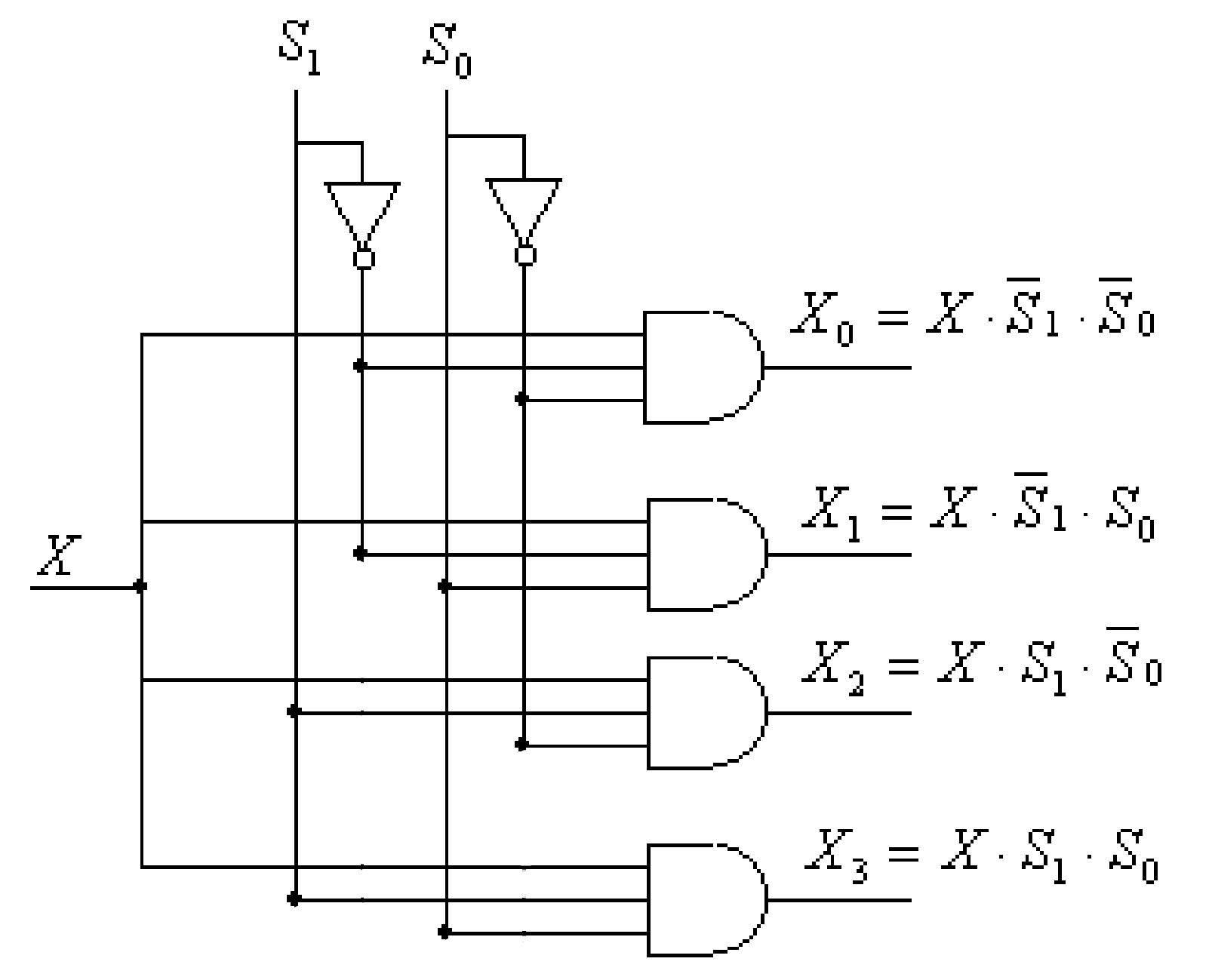
A demultiplexer performs the reverse process of multiplexer; it receives the information on a single line and steers to several output lines. Demultiplexer can also be called the Data Distributor as it can transmit the same data to the different lines. It transmits the data to \(2^N\) output lines, for which the select terminals of \(N\) bits are required. For example, to transmit the single data to four output lines (1:4 DMUX), select terminals of two bits are required; similarly for 1:8 DMUX select terminals of 3 bits are required and so on. The functional block diagrams of 1:4 DMUX and 1:8 DMUX are shown in figures.
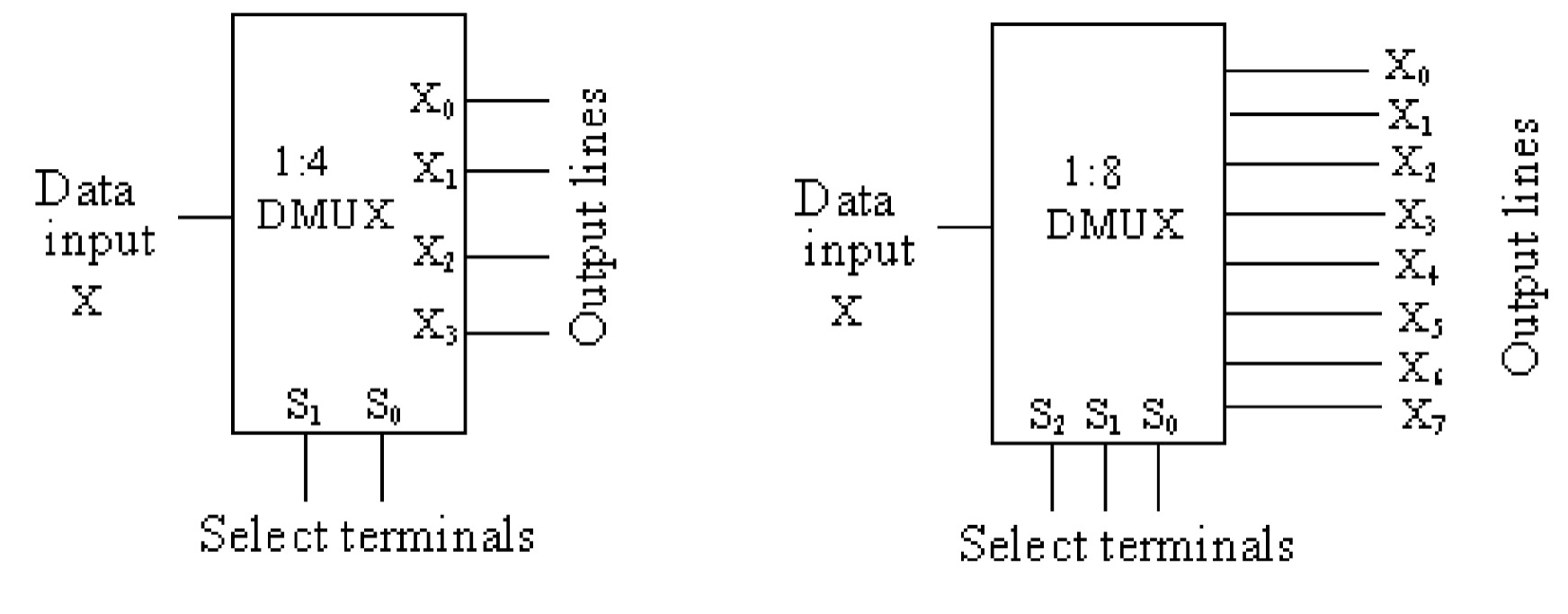
In a 1:4 DMUX, let \(X\) is the data input which is to be steered to 4 output lines \(X_0\), \(X_1\), \(X_2\), \(X_3\); the select terminals are (S_1),(S_0).
- If \(S_{1}\)\(S_{0}\) = \(00\) , the input data \(X\) will be go to the output \(X_0\).
- If \(S_{1}\)\(S_{0}\) = \(01\) , the input data \(X\) will be go to the output \(X_1\).
- If \(S_{1}\)\(S_{0}\) = \(10\) , the input data \(X\) will be go to the output \(X_2\).
- If \(S_{1}\)\(S_{0}\) = \(11\) , the input data \(X\) will be go to the output \(X_3\).
The Boolean expressions for \(X_0\), \(X_1\), \(X_2\), \(X_3\) are given by:
\[X_0 = X.\overline{S_1}.\overline{S_0}\] \[X_1 = X.\overline{S_1}.S_0\] \[X_2 = X.S_1.\overline{S_0}\] \[X_3 = X.S_1.S_0 \]The implementation of these functions (or 1:4 DMUX) can be done as shown in figure.