Diode
A Diode is a two-terminal, passive, non-linear device that can control voltage and current in a circuit. Some diodes are used primarily to rectify alternating current, some are used as signal detectors, and others are used as voltage references or voltage regulators. There are also optical diodes that are used as indicators (light-emitting diodes, or LEDs), signal sources (LEDs and laser diodes), or optical detectors (avalanche photodiodes and PIN diodes). The shape of a diode's current-voltage relationship determines its specific application, which in today's solid-state devices depends on how it is doped during manufacture. There are several classes of diodes besides the 'ordinary' rectifier, but of these, we shall examine only Schottky diodes, zener diodes, and light-emitting diodes.
Junction diodes
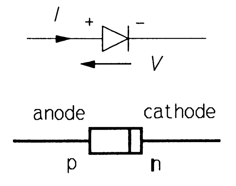
Junction diodes depend on \(p-n\) junctions in semiconductors for their operation. They are primarily used for rectification and signal detection, though they can also be used for voltage limitation or regulation. The symbol for an 'ordinary' diode is shown in figure \(1\). The \(n\)-type side of the \(p-n\) junction is the called the cathode (marked on the device often by a coloured band) and the \(p\)-type side is the anode. Forward current is said to flow when the direction of positive (conventional) current flow is from anode to cathode.
The current-voltage relation for a junction diode is given by the rectifier equation
\[I = I_{s}\left[exp\left(\frac{qV}{\eta k_{B}T}\right) - 1\right]\]
where \(V\) is the potential across the diode, positive if forward biased and negative if reverse biased and \(\eta\) which lies between \(1\) and \(2\). \(I_{s}\) is the reverse saturation current (a very small quantity), \(q\) is the magnitude of the electronic charge (\(1.6 \times 10^{-19} C\)), \(k\) is Boltzmann's constant (\(1.38 \times 10^{-23} J/K.\)) and \(T\) the absolute temperature in K. Putting in the values of \(q\), \(k\) and \(T\) (\(290\) \(K\)), equation 1 is approximately, for forward currents
\[I = I_{s}exp(40V)\]
The \(-1\) in equation 1 has been neglected as at normal forward voltages it is negligible. When the diode is reverse biased, \(V\) is negative and equation \(1\) reduces to
\[I = -I_{s} = 0 \]
Because the \(V-I\) relationship in the rectifier equation is not linear (that is, not of the form
\[I= \alpha V + \beta\]
where \(\alpha\) and \(\beta\) are constants) diodes are non-linear devices.
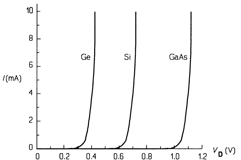
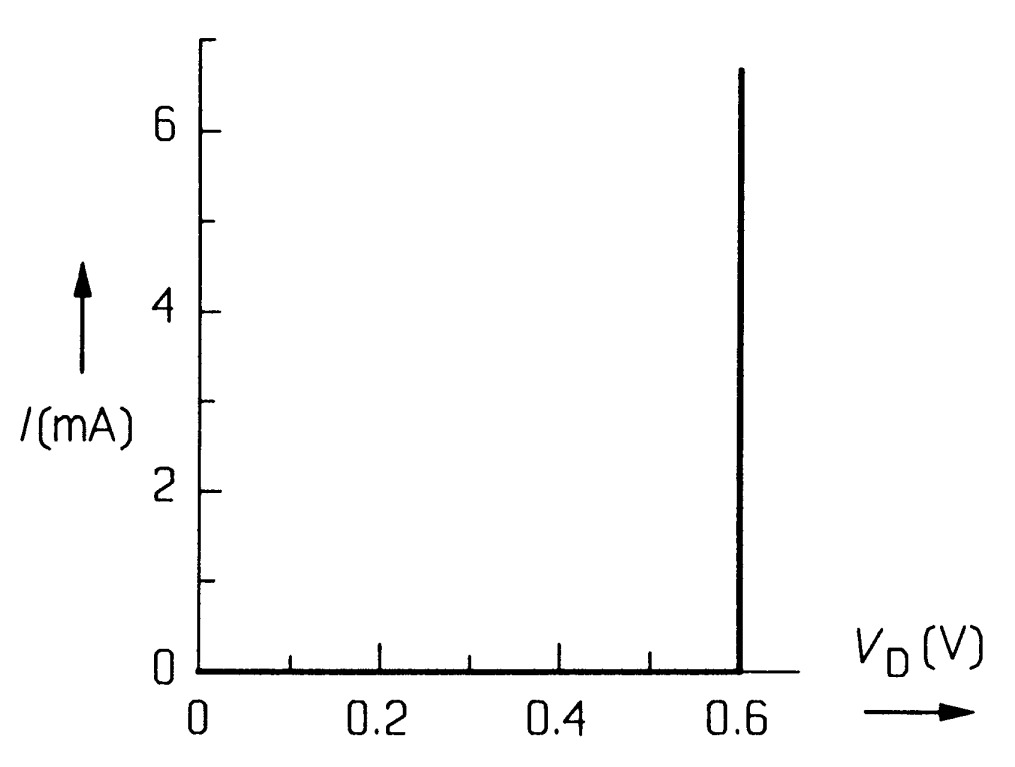
A graph of equation 1 at \(300\) \(K\) is drawn in figure 2 for different values of \(I_{s}\), corresponding to germanium, silicon and gallium arsenide signal (low current) diodes. On the scale of the graph the reverse current flow is negligible; it is also very dependent on temperature as well as the material of which the diode is made, and roughly doubles when the temperature rises by \(10\) \(K\). We see from figure 2 that the diodes conduct effectively only at a certain forward bias: \(0.3\) \(V\) for germanium, \(0.6\) \(V\) for silicon and \(1\) \(V\) for gallium arsenide diodes. Most common diodes have a forward drop of about \(0.6\) \(V\) and must therefore be made from silicon. The increase in current when the forward voltage rises above \(0.6\) \(V\) is very steep as expected from equation 4, though in an ideal silicon diode (figure 3) it would be vertical.
Although the rectifier equation does not indicate the fact, there is a reverse voltage, \(V_{b}\), dependent principally on the dopant concentration, where a diode will break down. Reverse breakdown in normal \(p-n\) junction diodes is usually irreversible, and damages the diode. Roughly speaking, the cost of a junction diode depends on how much current it can carry (which depends on the size of the active semiconductor material) and the voltage it can withstand in reverse bias: low-current, low-reverse-voltage diodes are very cheap and high-current, high-reverse-voltage diodes are dear.
There are, however, other parameters of interest in diodes than \(V_{RRM}\) (the reverse, repetitive, maximum voltage rating) and \(I_{F(AV)}\) (the average maximum forward current rating), such as the junction capacitance, the reverse recovery time, the surge current rating and the leakage current. A \(p-n\) junction diode stores charge in the depletion region near the junction and this charge must be removed rapidly at high frequencies, or the diode does not work properly. The time taken for the charge to dissipate when the reverse voltage is reduced to zero is called the reverse recovery time, \(t_{rr}\) and can vary from \(10\) \(ps\) down to \(1\) \(ns\). Roughly, the maximum operating frequency for a diode will be \(1/2\pi t_{rr}\). Diodes that operate in the UHF and VHF regions (\(50\) \(MHz\) up) are usually Schottky-barrier devices that recover instantly.
The junction capacitance depends on the area of the junction and the width of the depletion region:
\[C_{j}=\epsilon_{r}\epsilon_{0} \frac{A}{x_{j}} \]
where \(\epsilon_{r}\) is the relative permittivity (12 for silicon), \(\epsilon_{0}\) is the permittivity of a vacuum (\(8.85 \times 10^{-12} F/m\)), \(A\) is the junction area and \(x_{j}\) is the width of the depletion region. \(x_{j}\) is proportional to \(\sqrt{V_{i}}\), where \(V_{i}\) is the reverse voltage across the junction, so the capacitance decreases as the bias becomes more negative.
Taking a small signal diode, where \(x_{j}\) = \(10\) \(pm\) and \(A\) = \(2 \times 10^{-7}\) \(m^{2}\), we find \(C_{j} = 2\) \(pF\), about the right order of magnitude. Varactor and varicap diodes have a relatively large capacitance (\(100\) \(pF\) at \(V_{i}\) = \(0\)) that can be varied (as much as tenfold) by altering the reverse bias. They are used in circuits whose frequency of oscillation or resonance is voltage controlled. In forward bias the diode's capacitance is largely diffusion capacitance, which depends principally on the current flowing.
The rectifier equation enables us to calculate the dynamic resistance (or AC resistance), \(r_{d}\), of all (be they made from silicon, germanium, gallium phosphide or any other material) junction diodes when forward biased:
\[r_{d} = \frac{dV}{dI} = \left(\frac{dI}{dV}\right)^{-1}\]
Differentiating equation 1,
\[ \left(\frac{dI}{dV}\right)=\left(\frac{q}{k_{B}T}\right)I_{s}exp\left(\frac{qV}{k_{B}T}\right)=\left(\frac{q}{k_{B}T}\right)=40~I \]
This is at room temperature (\(300\) \(K\)), so that \(r_{d} =0.025/I\), or about \(1\) \(\Omega\) when the forward current is \(25\) \(mA\). However, when the current falls to \(1\) \(mA\), \(r_{d}\) is \(25\) \(\Omega\), which is not inconsiderable. For a forward current of \(25\) \(mA\), the voltage drop, \(V_{D}\), according to equation 2 (taking \(I_{s}\) as \(1\) \(pA\), typical for a silicon signal diode) will be \(0.60\) \(V\). For \(I= 1\) \(mA\) we find \(V_{D}\) is \(0.52\) \(V\) and if \(I= 1\) \(A\), \(V_{D}\) is \(0.69\) \(V\); a forty-fold increase in current has resulted in only a \(15 \%\) increase in the voltage across the junction. As \(V_{ D}\) is almost constant a diode can be modelled as a voltage source in series with \(r_{d}\).
Example 1 In the circuit of figure 4a, what will the current flow if the diode requires a forward bias of \(0.6\) \(V\) to pass a forward current of \(25\) \(mA\) and \(V_{s}= 1 + 0.01~sin \omega t\) volts?
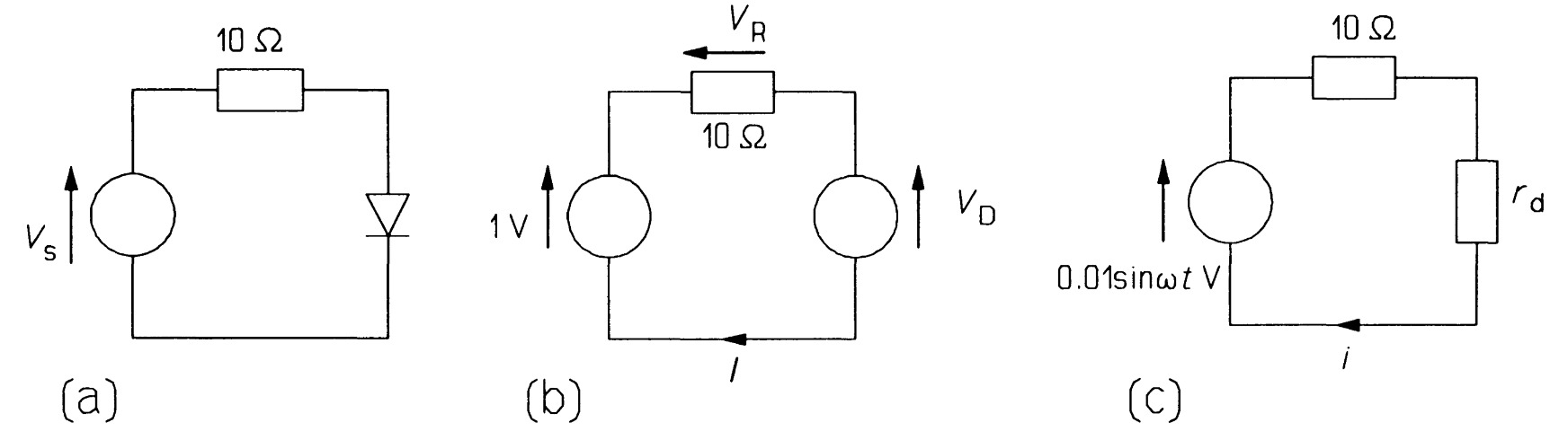
The voltage source can be split into two, and we can use the superposition theorem, provided that the alternating component is small compared to the direct. Taking the direct part first and neglecting \(r_{d}\), we have the circuit of Figure 4b. From Kirchhoff's voltage law,
\[V_{R} + V_{D} = 1\]
so as \(V_{D} =\) \(0.6\) \(V\), \(VR = 0.4\) \(V\), leading to a current of \(40\) \(mA\) by Ohm's law. As the current is a little more than \(25\) \(mA\) we can refine our value of \(V_{D}\)
\[V_{D} = r_{d}~\Delta I = 1 \times (40- 25) = 15~ mV\]
\(V_{D}\) must be \(>\) \(0.6\) \(V\) as \(I~>\) \(25\) \(mA\), so \(V_{D} = 0.615\) \(V\). But this means that the voltage across the \(lO\) \(\Omega\) resistance is \(15\) \(mV\) less at \(0.385\) \(V\), and the direct current is reduced to \(38.5\) \(mA\).
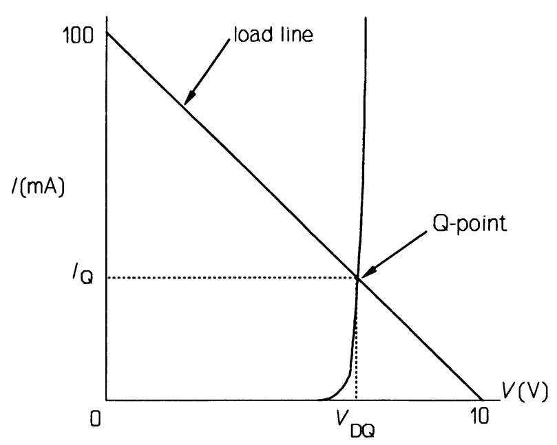
Load lines
By Kirchhoff's voltage law in the circuit of figure \(4b\)
\[V_{s} = V_{R} + V_{D} = IR + V_{D}\]
Rearranging, (8) where \(V_{s}\) is the source voltage. If this equation is plotted on a graph of current as a function of \(V_{D}\), it results in a straight line of slope \(-1/R\) and intercept on the \(I-\)axis of \(V_{s}/R\), as in figure 5. The load line is the locus of all possible values for the diode forward drop, \(V_{D}\), no matter what the diode. If the diode characteristic is plotted too, the intersection of the load line occurs at the quiescent point or \(Q\)-point so that the diode's quiescent voltage (\(V_{DQ}\)) and current, \(I_{Q}\), can be read off the axes. We shall find load lines very useful where transistor circuits are concerned.
We can now take the \(0.01~sin~\omega t\) \(V\) source independently. The diode operates at a \(V_{DQ}\) bias, \(0.615\) \(V\), and \(I_{Q}\) , \(38.5\) \(mA\). The alternating source will induce small changes in current and voltage about the \(Q\)-point, which we can find by a linear approximation using the diode's dynamic resistance, \(r_{d}\). The value of \(r_{d}\) must be calculated from
\[r_{d} = \frac{0.025}{I_{Q}} = \frac{0.025}{0.0385} = 0.65 \Omega\]
and the AC circuit is as in figure 4c. The current by Ohm's law is given by
\[i = \frac{0.01~sin~\omega t}{10.65} = 0.94~sin~\omega t ~~mA\]
Direct and alternating currents can be added for a total current of (\(38.5 + 0.94~sin~\omega t\)) \(mA\). Using equation 1 to give an 'exact' solution is pointless since the accuracy of this approximation is about \(1 \%\). Were the temperature of the diode to increase to \(100 ^{\circ}C\), a not uncommon occurrence, then \(I_{s}\) would increase by about \(2^{7·3}\) (because the temperature has increased \(73\) \(K\) and \(I_{s}\) doubles every \(10\) \(K\)) or about \(160\) times, while \(q/k_{B}T\) would decrease to \(32\). \(r_{d}\) would increase to \(0.031/I\), or about \(1.24\) \(\Omega\) at \(25\) \(mA\). The increase of \(0.24\) \(\Omega\) is only \(2 \%\) of the circuit's total resistance; accordingly, the solution is little affected even though \(I_{s}\) increased dramatically and \(r_{d}\) significantly.
Schottky diodes
A metal-semiconductor contact can be non-rectifying (or ohmic) and rectifying: Schottky diodes (sometimes called Schottky-barrier diodes) use the rectifying properties. Usually, the metal is aluminum (or, rarely, gold), and the semiconductor is silicon (occasionally germanium). Figure 6 shows a Schottky diode and its circuit symbol. Schottky diodes rely on majority-carrier conduction - unlike \(p-n\) junction diodes, which rely on minority-carrier conduction - so they do not store charge at the junction. Consequently, they can change very fast from conducting to non-conducting states and are used in circuits that must switch on and off rapidly, such as switch mode power supplies (\(q.v.\)). The original cat's whisker detector of the early radio years depended on the rectifying properties of a metal-semiconductor contact. They were notoriously unreliable (though point-contact diodes continued to be manufactured until quite recently) and so came to be replaced by vacuum-tube devices, which in turn were replaced by semiconductor devices once more, based on the new technology and understanding of solid-state physics brought about in the \(1930s\) and \(1940s\).
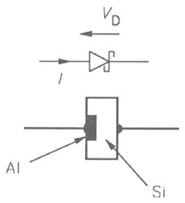
When a metal forms contact with a semiconductor, a potential barrier is set up at the interface. At moderate to low dopant densities in \(n\)-type silicon (\(\leq 10^{23}\) atoms per \(m^{3}\)), electrons pass from semiconductor to metal over this barrier by a thermionic emission process. If the metal is made positive to the semiconductor (forward bias), the barrier height is reduced, and if reverse bias is applied, it is increased. The current flow follows equation \(1\) again. However, \(I_{s}\) is now given by
\[I_{s}=A_{j}A^{*}T^{2}~exp\left(\frac{-q\phi_{B}}{k_{B}T}\right)\]
which known as Richardson's equation. \(A_{j}\) is the area of the contact, \(A^{*}\) is the effective Richardson constant(\(= 10^{8}\) \(NK^{2}/m^{2}\) for \(n\)-type silicon), \(\phi_{B}\) is the barrier height in volts and the other symbols have their usual significance. \(I_{s}\) works out to about \(16\) \(\mu A\) for a \(1\) \(mm^{2}\) contact when \(\phi_{B}\) is \(0.7\) \(V\) as it is for aluminum and \(n\)-type silicon.
The Richardson's constant depends on the effective mass of the semiconductor material contacting the metal such that it can be expressed by:
\[ A^{*}= 4 \pi q m^{*} \frac{k^{2}}{h^{3}}\]
where \(q\) is the electron charge, \(m^{*}\) is the effective mass of the semiconductor making contact with the metal. \(m^{*}\) of your material is obtained from literature or must be calculated, \(k\) Boltzmann constant and \(h\) the Planck's constant.
As a result of this high value of \(I_{s}\) (about \(2 \times 10^{6}\) times as large as for a \(p-n\) junction diode), the forward drop across a conducting Schottky diode can be much smaller than for a \(p-n\) junction diode.
For example, a Schottky diode having a \(1\) \(mm^{2}\) \(Al-Si\) contact with \(I.\) \(= 16\) \(\mu A\) will conduct \(25\) \(mA\) at a forward bias of only \(0.2\) \(V\). Of course, the penalty to be paid is the relatively large reverse (leakage) current of \(16\) \(\mu A\) at \(0\) \(V\). In practice, the requirements for rectifying power Schottky diodes are different from those of fast-switching signal diodes so that the contact metal may be different: chromium, platinum and tungsten are all used. In integrated circuit manufacture, aluminum is preferred as it is easily evaporated. The \(1N6263\) RF Schottky diode has a reverse breakdown voltage of \(60\) \(V\) (at \(10\) \(\mu A\)), a maximum capacitance of only \(2.2\) \(pF\), and a switching time of a few picoseconds, with a forward voltage drop of only \(0.3\) \(V\) at \(I_{F}\) \(= 1\) \(mA\). The capacitance of the diode is in parallel with it, so will short it out at high frequencies.
To summarise, Schottky diodes have similar current-voltage characteristics to \(p-n\) junction diodes: the difference lies chiefly in their faster switching times and, in some cases, their reduced forward voltage drops, advantages that must be set against their much larger reverse currents.
Zener diodes
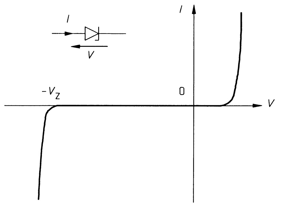
The symbol for the Zenor diode and its current-voltage relationship is shown in the figure.
The zener diode is designed to be used and to break down in reverse bias but in a controlled fashion so that the process is reversible and not destructive. Zeners can be readily brought with zener voltages from \(204\) \(V\) to \(270\) \(V\), but the spread in the breakdown voltage from the nominal values is usually about \(\pm 5 \%\). In the forward bias, the silicon zener diode conducts at \(0.6\) \(V\), just the same as the normal silicon diode. The breakdown process in reverse bias in a normal \(p-n\) junction diode is caused by an avalanche effect: electrons are accelerated in the junction region by the very high fields (as much as \(1\) \(GV/m\)) to such a high speed that they can remove bound electrons. In turn, these electrons will be accelerated by the applied field to produce more electrons by the same process. The result is an avalanche of current.
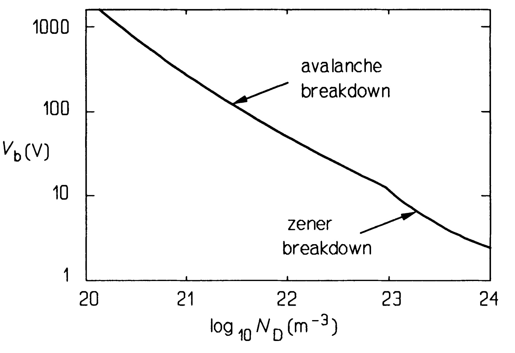
In low-voltage zener diodes, this is not the process by which breakdown occurs, though it is in 'zener diodes' with breakdown voltages above the \(6\) \(V\). Low-voltage zener diode breakdown by a tunneling process called zener breakdown, in which electrons in the valance band find themselves close to empty states in the conduction band so that they can tunnel through the band gap between them, even though they do not possess the necessary energy, classically. This process can only work if there is close physical proximity of electron and empty state in the conduction band, which in practice means if the doping density is high on the \(p\)-side. In fact, the doping density in silicon must be about \(10^24\) \(atoms/m^3\) for the \(V_Z\) of \(2\) \(V\). As the doping levels are reduced, there is less and less tunneling and more and more avalanche breakdown: at a dopant density around \(3 \times 10^23\) \(atoms/m^3\), the two processes contribute equally.
The dynamic resistance of zener diode in reverse breakdown is at a minimum around a zener voltage of \(7 V\) (where it may be about \(10\) \(\Omega\) for a current of \(5\) \(mA\)), rising substantially as the zener voltage drops to as much as \(100\) \(\Omega\) for a \(5\) \(mA\) current in a \(3\) \(V\) zener, and also as the zener voltage rises to about \(100\) \(\Omega\) again for a \(5\) \(mA\) current and \(V_Z = 270\) \(V\). In addition to this drawback, when \(V_Z\) is greater than about \(7\) \(V\), it has a large temperature coefficient, \(\theta_{VZ}(= V_Z^{-1}\Delta V_{Z}/\Delta T)\), of about \(+0.1\) \(\%/K\). To some extent, this can be offset by connecting forward-biased \(p-n\) junction diodes in series with the zener, as these have negative temperature coefficients. When \(V_{Z}\) falls below about \(5\) \(V\), \(\theta_{VZ}\) becomes negative. Despite all their deficiencies, zeners are a cheap and reasonably effective way of achieving voltage regulation and voltage reference.
Example 2
An example of a simple current-regulating circuit is shown in figure 9. In this circuit \(V_{z} = 20\) \(V\) at a current of \(10\) \(mA\), when \(r_{d}\) = \(20\) \(\Omega\). The load current desired is \(15\) \(mA\), while the supply voltage varies from \(35\) to \(40\) \(V\). Given that \(R_{s}\) = \(600\) \(\Omega\), calculate the percentage regulation of the load current. What is the power dissipated in the load, the zener diode, and the whole circuit when \(V_{s} = 35\) \(V\) and when \(V_{s}\) \(= 40\) \(V\)?
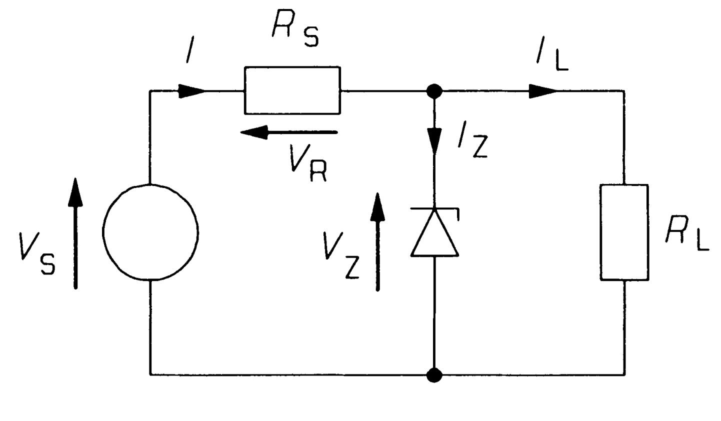
The load must be given by \(V_{Z}/I_{L}\) = \(20/0.015 = 1.333\) \(k\Omega\). Since \(V_{R} = V_{s} - V_{Z}\) by Kirchhoff's voltage law, we can see that
\[V_{Rmin} = 35 - 20 = 15 V\], and so
\[I_{min}= 15/600 = 25 mA.\]
In a like manner,
\[I_{max} = V_{Rmax}/600 = (40- 20)/600 = 33.3 mA.\]
Now, by Kirchhoff's current law, \[I= l_{Z} + I_{L}\], thus when \(I= I_{min}= 25\) \(mA\), \(I_{Z} = 10\) \(mA\) since \(I_{L} = 15\) \(mA\). This is the rated value, so then \(V_{Z} = 20\) V. When \(I= I_{max}\), \(I_{Z} = 33.3 - 15 = 18.3\) \(mA\), which is \(8.3\) \(mA\) greater than the rated current. \(V_{Z}\) must, therefore, be greater than \(20\) \(V\) by an amount given by
\[ \Delta V_{Z} = \Delta I_{Z}r_{d} = 8.3 \times 20 = 166 mV \]
Thus, the voltage (and load current) regulation is
\[\frac{V_{Zmax} - V_{Zmin}}{V_{Z}} \times 100 \% = \frac{20.166 - 20}{20} \times 100 \% = 0.83 \% \]
Had we also considered the effect of temperature variations, the result would have been less good; nevertheless, the performance of the zener is credible.
The power dissipation in the circuit when \(V_{s} = 35\) \(V\) is
\[ V_{s}I_{min} = 35 \times 25 = 875 mW \]
The zener's power dissipation is
\[V_{Z}I_{Z} = 20 \times 10 = 200 mW \]
and the load's power dissipation is
\[20 \times 15 = 300 mW\].
When \(I= I_{max}\), the source supplies \(40 \times 33.3 = 1.33\) \(W\), to the circuit.
The load power is
\[V_{Z}^{2}/R_{L} = \frac{20.1662}{1333} = 305 mW\]
\(5\) \(mW\) more than before, as the zener voltage has increased by \(0.166\) \(V\). The zener's dissipation is \(20.166 \times 18.3 = 369\) \(mW\), up \(169\) \(mW\) from its minimum value: it rises quite sharply as the source voltage increases.
Light-emitting diodes (LEDs)
In a forward-biased \(p-n\) junction diode, majority carriers either side of the junction move in opposite directions and cross the junction, becoming minority carriers on the other side. The process is called minority-carrier injection and the density of minority carriers is thereby increased near the junction. However, majority carriers will combine with the injected excess minority carriers and re-establish equilibrium. The recombination process can produce a photon, a radiative recombination, and ideally one would like all such recombinations in a LED to be radiative, that is for the quantum efficiency to be 100%, but in fact quantum efficiencies are much lower, ranging from about \(0.1 \%\) to \(10 \%\), depending on the structure of the valence and conduction bands. In materials where the band gap is direct, a charge carrier can recombine without changing its momentum, but in indirect-gap materials a change of carrier momentum requires a phonon (quantum of lattice vibrational energy) to participate. The probability of a radiative recombination is thereby much reduced in indirect-gap materials.
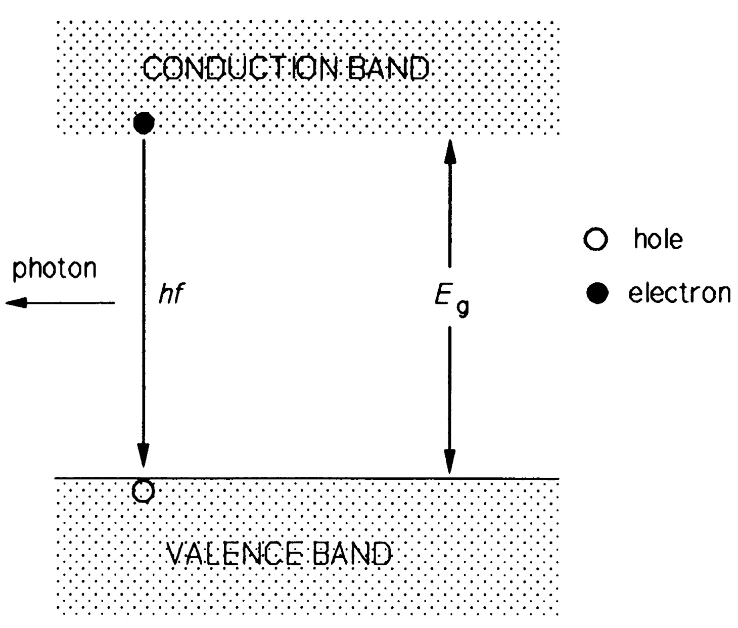
Figure 12 shows radiative recombination of an electron with a hole and a hole with an electron in a LED.
The photon (quantum of light energy) emitted has an energy very close to the gap energy, \(E_{g}\), so that the frequency of the emitted light is given by
\[E = hv = \frac{hc}{\lambda}\]
where \(h\) is Planck's constant (\(6.627 \times 10^{-34} Js\)), \(c\) the speed of light in a vacuum (\(3 \times 10^{8} m/s\)) and \(\lambda\) is the wavelength in a vacuum of the light emitted. In fact the most probable energy of the photon is a little larger than this, by about \(k_{B}T\):
\[ \frac{hc}{\lambda} = E_{g} + k_{B}T \]
\[\lambda = \frac{hc}{(E_{g} + k_{B}T)}\]
Thus the wavelength of the light is largely determined by the bandgap of the material. Table \(1\) gives some properties of a few semiconducting materials. Generally speaking, the higher the melting point, the more difficult they are to fabricate into devices. Despite the wavelength of \(GaP\) bandgap emission being in the yellow-green region, it is used to make red LEDs by doping it with zinc and oxygen, and green LEDs by doping with nitrogen. The energies of the photons emitted range over about \(3k_{B}T\) and it can be shown that the linewidth (the range of wavelengths emitted) of the LED, \(\Delta\lambda\), is given by
\[\Delta\lambda= 2.4k_{B}T\lambda^{2}\]
where \(\Delta\lambda\) and \(\lambda\) are in \(\mu m\) and \(k_{B}T\) is in \(eV\).
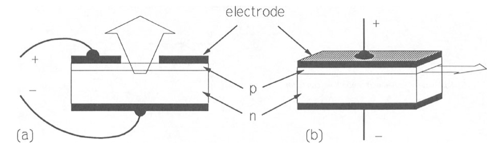
For example in a red LED the emission is at \(0.65\) \(\mu m\), so at \(300\) \(K\) where \(k_{B}T\) is about \(0.025\) \(eV\), the linewidth is about \(2.24 \times 0.652 \times 0.025 = 0.024\) \(pm\) (\(24\) \(nm\)). The linewidth does not matter if the LED is an indicator lamp, but has an important bearing on their use as fibre-optic communications sources. The narrower linewidths of semiconductor lasers makes them much more suitable for this purpose. LEDs are designed to emit light from the top surface, while signal LEDs are designed to emit in the plane of the \(p-n\) junction as shown in figure 13. The latter mode of emission is known as edge emission. It results in a greater concentration of the light which increases the amount coupled into an optical fibre.
Table 1 Properties of some semiconducting materials
| Substance | Group in Periodic Table | Melting Point (K) | \(E_{g}\) (\(eV\)) | \(\lambda\) (\(nm\)) |
|---|---|---|---|---|
| C | IV | 4300 | 5.4 | 230 (UV) |
| Si | IV | 1683 | 1.11 | 1100 (IR) |
| Ge | IV | 1210 | 0.66 | 1810 (IR) |
| P-SiC | IV-IV | 3070 | 2.3 | 534 (green) |
| AlAs | Ill-Y | 1870 | 2.16 | 568 (yellow-green) |
| AlSb | Ill-Y | 1330 | 1.60 | 764 (IR) |
| GaP | Ill-Y | 1750 | 2.24 | 548 (green) |
| GaAs | Ill-Y | 1510 | 1.43* | 854 (IR) |
| InP | Ill-Y | 1330 | 1.35* | 903 (IR) |
| a.-SiC | IV-IV | 3070 | 2.86 | 431 (blue-violet) |
| ZnS | II-VI | 2100 | 3.67* | 336 (UV) |
| ZnSe | II-VI | 1793 | 2.58* | 477 (blue) |
| CdS | II-VI | 1748 | 2.42* | 508 (green) |
| CdSe | II-VI | 1512 | 1.74* | 704 (deep red) |
| CdTe | II-VI | 1200 | 1.44* | 848 (IR) |
Notes: * = direct-gap material. Wavelengths of colours are: blue - \(470\) \(nm\), green - \(520\) \(nm\), yellow -\(580\) \(nm\), orange - \(600\) \(nm\), red \(650\) \(nm\).
Applications for diodes
There are so many applications for diodes that we can only look at a few typical uses.
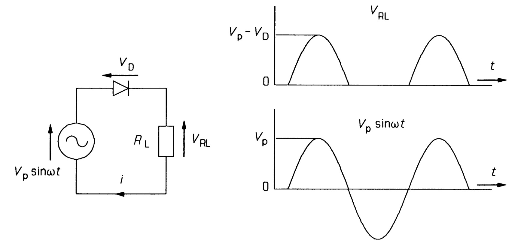
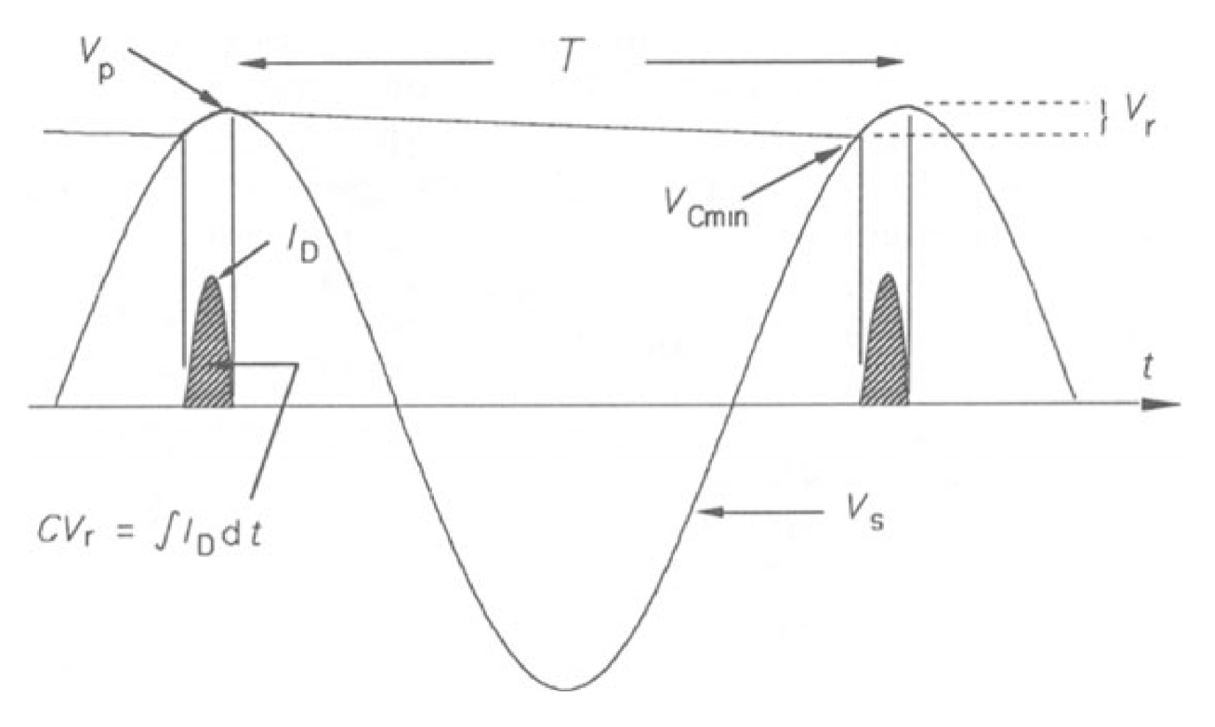
The half-wave rectifier
The half-wave rectifier is shown in figure 14, together with the voltage waveform across \(R_{L}\) Though the current is unidirectional, it varies from zero to a maximum of \((V_{P} - V_{D} )/R_{L}\) since by Kirchhoff's voltage law,
\[v_{L} = V_{P}sin\omega t- V_{D}\]
By adding a capacitor to the circuit as in figure 15, we can smooth the current flow through \(R_{L}\). During the positive half cycle, while the diode conducts, the capacitor charges up, so that it supplies current when the diode is not conducting. Suppose \(V_{P} \geq\geq V_{D}\), so that the load charges up very nearly to \(V_{P}\) volts. As the voltage drops from its peak value the capacitor discharges according to
\[V_{Cmin}=V_{P}~exp~\left(\frac{-t}{R_{L}C}\right)\]
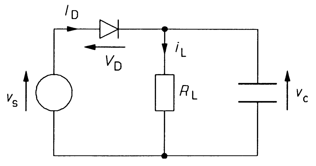
Then when the applied voltage increases to \(V_{Cmin}\) the capacitor begins to charge again as in figure 16. The time during which the capacitor discharges is almost one period, \(T (= 1/f)\), so if \(T \leq\leq R_{L}C\), the time constant, the exponential decay is approximately a straight line:
\[V_{Cmin}=V_{P}\left(1-\frac{T}{R_{L}C}\right)=V_{P}\left(1-\frac{1}{R_{L}Cf}\right)\]
(as \(e^{-x}= 1 - x\) for small \(x\)). T has been replaced by \(1/f\), assuming that the charging time is negligible. The capacitor now charges up almost to \(V_{P}\) once again. The difference between maximum (\(V_{P}\)) and minimum voltage is the ripple voltage, \(V_{r}\), which is
In many texts the ripple voltage is defined as the r.m.s. value of the alternating component. For a half-wave rectifier with little ripple so that the alternating component is almost a saw-tooth wave, the r.m.s. ripple would be \(V_{r}/2\sqrt{3}\). But for other ripple waveforms, the conversion factor would be different. Since one normally measures peak-peak ripple, it seems preferable to define this as \(V_{r}\).
\[V_{r} =V_{P}-V_{Cmin}=V_{P}-V_{P}\left(1-\frac{1}{R_{L}Cf}\right)\]
Or,
\[V_{r}=\frac{V_{P}}{R_{L}Cf}\]
Example 4
Suppose we wish to smooth the output of a half-wave rectifier operating at \(50\) \(Hz\) with \(R_{L}\) = \(100\) \(\Omega\), \(V_{p}\) = 340 V, so that the peak-to-peak ripple is \(2%\) of \(V_{p}\), what must \(C\) be? A ripple of \(2 \% \) means that \(V_{p}/V_{r} = 50\), and equation gives
\[C = \frac{V_{P}/V_{r}}{R_{L}f} = \frac{50}{100 \times 50} = 0.01 F\]
This is a fairly big capacitance. Because smoothing capacitances often need to be large they are normally electrolytic types, which occupy less volume for a given capacitance. The current supplied to the capacitor must be enough to charge it up by an additional amount \(V_{r}\). In the example given the capacitor charges up from \(0.98V_{P}\) to \(V_{P}\) (actually a little bit longer because after the peak of the supply voltage is attained the supply voltage drops more slowly than the capacitor would discharge). Thus the phase of the voltage waveform goes from \(sin-1 0.98\) to \(sin-1\) (or from \(78.5°\) to \(90°\)), which takes \((90 - 78.5)/360\) of one cycle, or \(0.032 \times 0.02\) \(s\), since one cycle is \(0.02\) \(s\). This is only 0.64 ms. Let us suppose the current pulse shape is square, then
\[i = C\frac{dv}{dt}=\frac{CVr}{\delta t} =\frac{0.01 \times 6.8}{6.4 \times 10^{-4}} = 106 A \]
If we assume a form factor of \(2/\pi\) for the current (taking it to be sinusoidal), the maximum current flow is magnified by \(\pi/2\) to \(167\) \(A\). However, this current is carried for only a very short time: the average diode current during one cycle (\(0.02\) \(s\)) is only \(3.4\) \(A\), and the diode need only have this current rating. The maximum energy stored in the capacitor is \(\frac{1}{2}CV_{P}^{2}\), or 578 J, and the minimum is \(\frac{1}{2}CVC_{min}^{2} = \)\(555\) \(J\), so only \(23\) \(J\) are supplied to the load every cycle, at a rate of \(23 \times 50= 1.15\) \(kW\), and this is the power dissipated in the load.
The full-wave rectifier
The half-wave rectifier in effect uses only half the supply. the full-wave rectifier uses all of the supply waveform and is therefore more readily smoothed and produced only half as much peak current flow into the smoothing capacitor as the half-wave rectifier. There are two ways principally of producing full-wave rectification:
- one uses a centre tapped transformer and two diodes,
- the other uses a bridge diode network.
In figure 17a, \(D_{1}\) conducts on the positive half-cycle, while \(D_{2}\) blocks. On the negative half-cycle \(D_{2}\) conducts while \(D_{1}\) blocks. Only half of the transformer secondary is used at a time, though it must still be wound for maximum current rating. A capacitor across the load must be used for smoothing, but need only be half of the capacitance of that used in a half-wave rectifier for the same ripple.
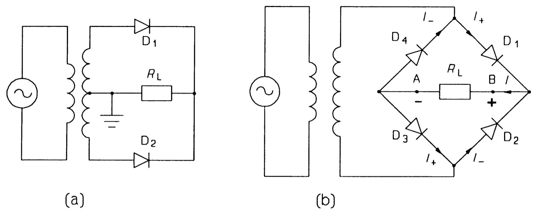
The bridge diode network circuit is shown in figure 17b. It works like this: on the positive-going waveform diodes \(D_{1}\) and \(D_{3}\) conduct as they are forward biased, while diodes \(D_{2}\) and \(D_{4}\) do not conduct as they are reverse biased. During the negative half-cycle, \(D_{2}\) and \(D_{4}\) are forward biased, so they conduct while \(D_{1}\) and \(D_{3}\) are reverse biased and do not conduct. The current flow on the positive half-cycle, \(I_{+}\), is from \(A\) to \(B\) through the load, \(R_{L}\), and so also is the current flow during the negative half-cycle, \(I_{-}\). A smoothing capacitor can be added as in figure 18a, with the current and voltage waveforms of figure 18b.
The analysis of the effect of this capacitor follows the same path as for the half-wave rectifier, and leads to \(\Delta V = V_{p}/2R_{L}Cf\), so the capacitance is halved for the same ripple, as is the charging current.
Nowadays plenty of 4-terminal diode bridges are available, ranging from the PCB mounted type \(DF02G\) supplied by General Instruments and rated at \(V_{RRM} = 200\) \(V\), \(I_{F(AV)} = 0.9\) \(A\). In most cases it is far cheaper to buy four diodes of the correct rating. \(5\)-terminal bridge rectifiers are available for use with \(3\)-phase supplies.
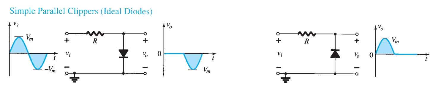
Clipping and clamping: voltage limitation
There are occasions on which one wishes to restrict the voltage at some point in a circuit, or to clip a waveform. Consider the circuit of figure 19; because the diode must drop \(0.6\) \(V\), \(V_{o}\) must always remain at \(5.6\) \(V\). Moreover, the current through the resistor must be (\(15 - 5.6)/470 = 20\) \(mA\). The diode has clamped \(V_{o}\) to \(0.6\) \(V\) above the voltage at the diode's cathode, and it does not matter what the supply voltage is, as long as it is more than \(5.6\) \(V\).
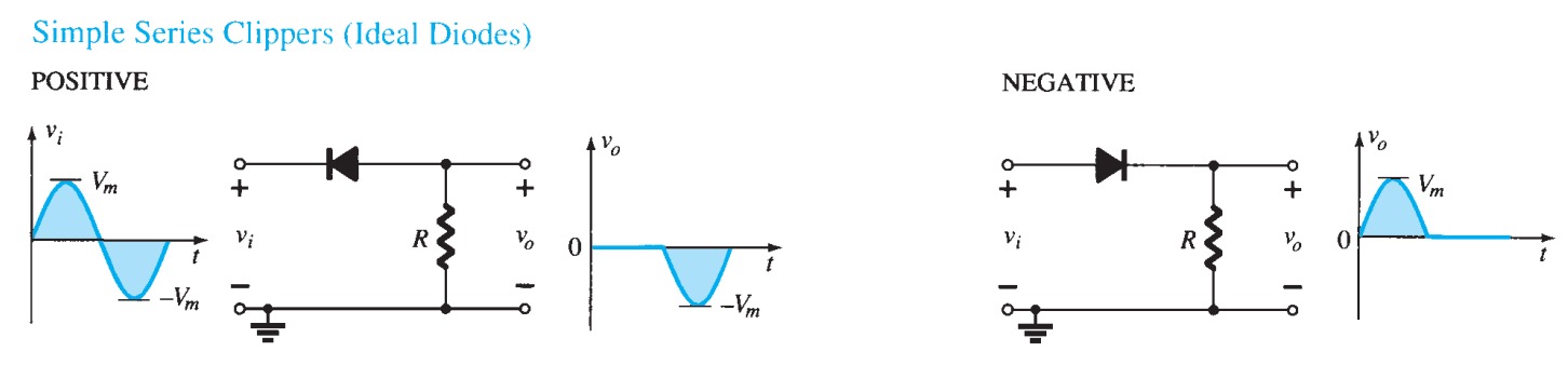
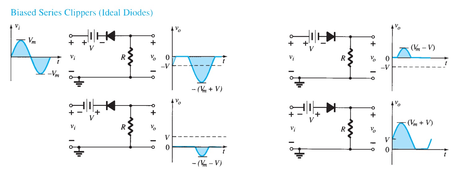
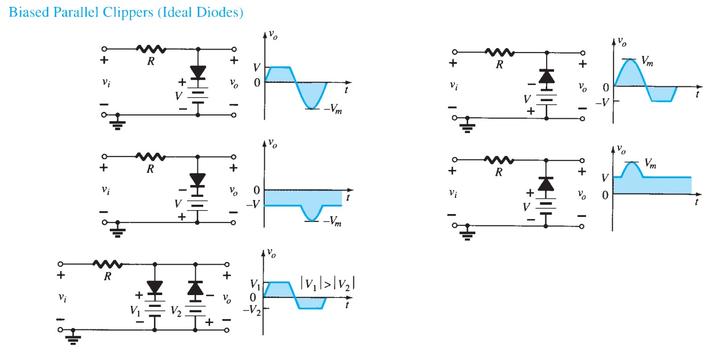
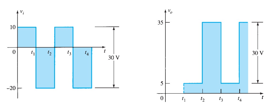
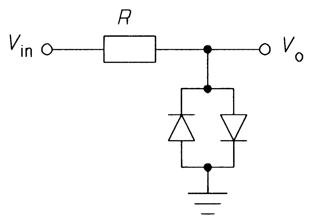
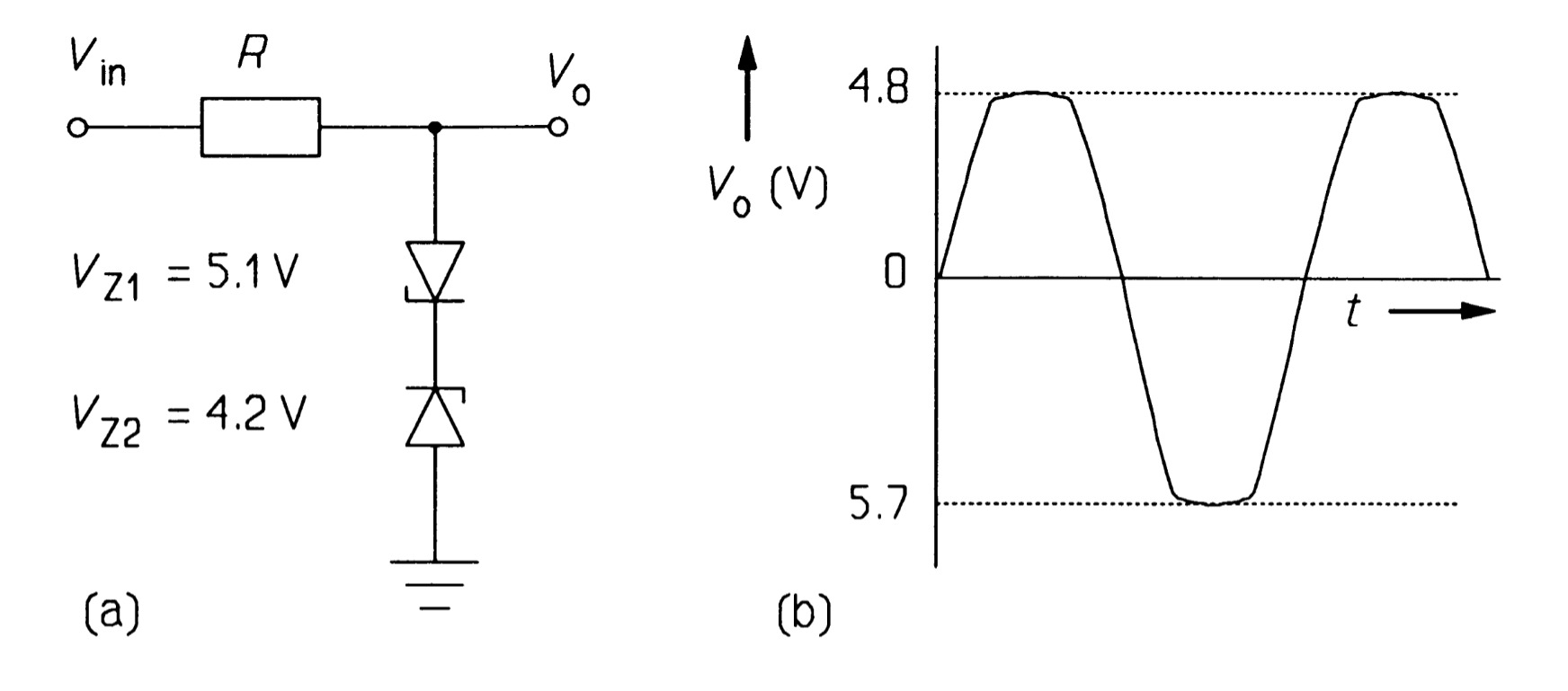
The circuit of figure 20 shows two diodes in use as voltage limiters to keep the input to the rest of the circuit between \(\pm 0.6\) \(V\). In cases where a waveform is to be clipped, two zeners can be put in series as in figure \(21a\), giving the waveform in figure \(21b\). The clipping voltage in this case is \(0.6\) \(V\) more than the zener breakdown because of the forward drop across the second zener.
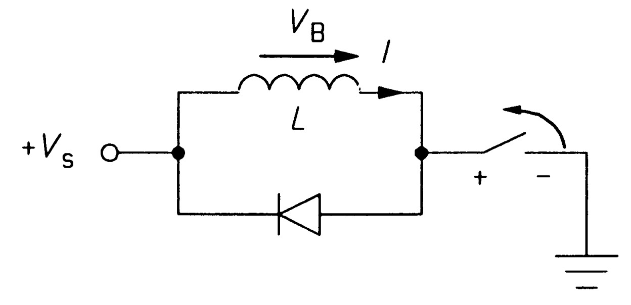
Inductive loads can sometimes give rise to problems when they are disconnected from their supply, as the voltages generated can damage the switch. A diode connected across the load as in figure \(22\) is the solution, though it is no use if the supply is AC, since the diode will short out half of the waveform. The voltage produced by the inductor will be \(V_{B} = Ldi/dt\), so if the supply is disconnected, \(di/dt\) is large and negative, and the voltage across the load is large and of opposite polarity to the supply. The diode then conducts and allows the load current to decay harmlessly.
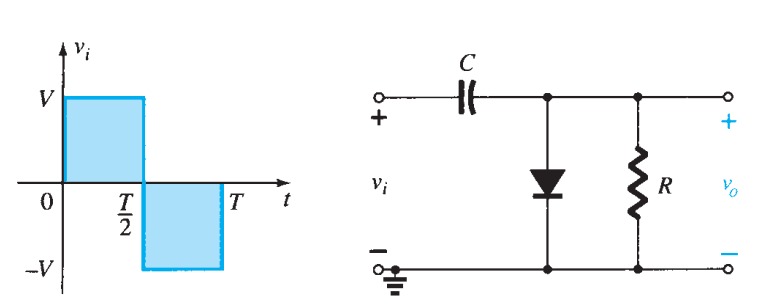
DC restoration
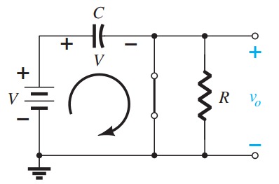
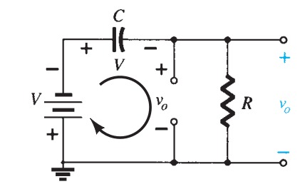
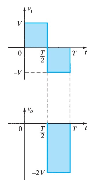
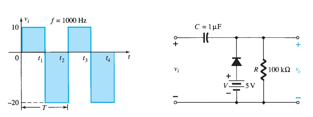
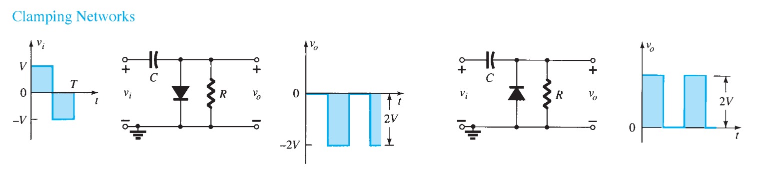
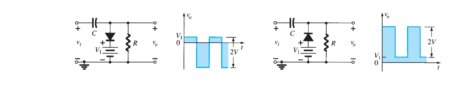
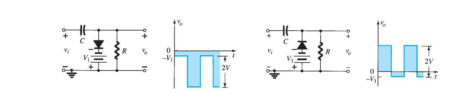
Capacitors are often used to couple circuits, in which case the direct component of the signal is lost, as capacitors block DC. The direct component of the signal can be restored, very nearly, by using a diode as shown in figure 23a.
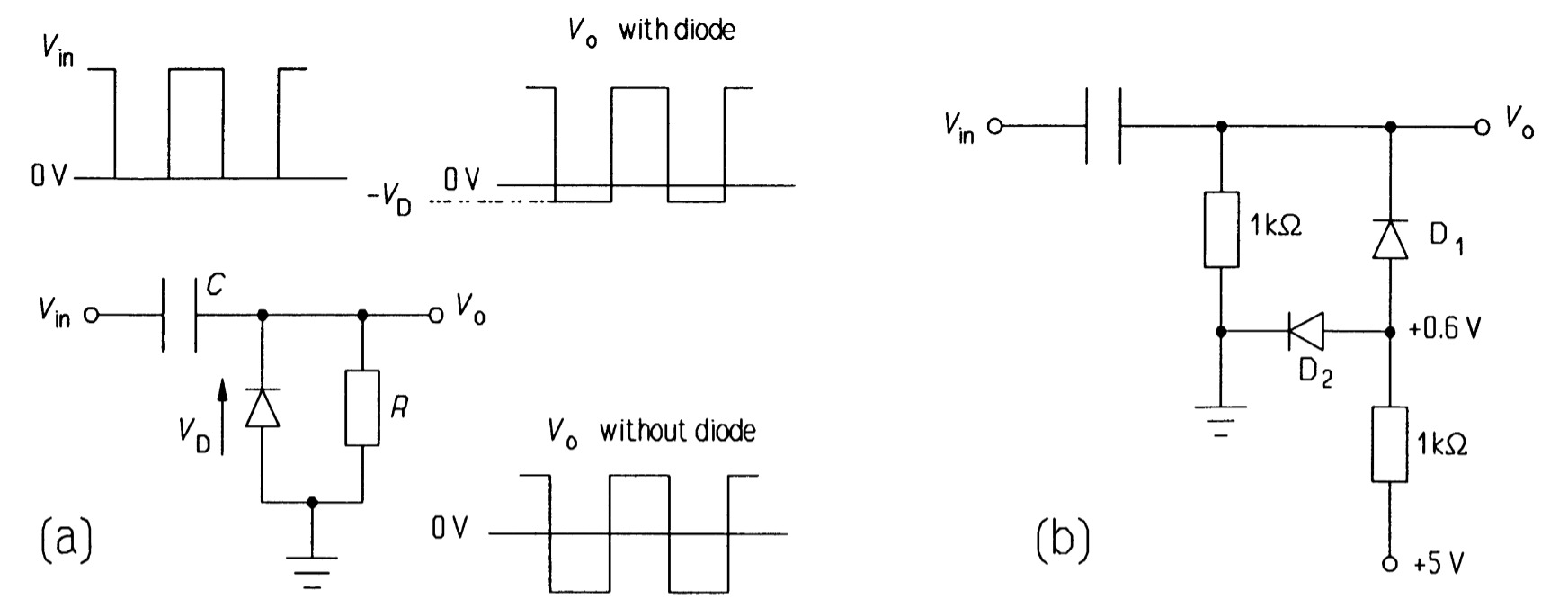
The input waveform is shown and the output waveforms with and without the diode. The reverse biased diode restores the direct component except for the \(0.6\) \(V\) diode forward drop. By using two diodes as in figure 23b, the signal is fully restored. The second diode holds the first diode's anode at \(+0.6\) \(V\), so the drop across the first diode brings the signal down to \(0\) \(V\). Compensation of this kind is essential of course for signals having amplitudes less than \(0.6\) \(V\). The use of a second identical diode rather than a voltage divider ensures that temperature effects are fully compensated.
Voltage multipliers
By using ingenious combinations of transformers, diodes and capacitors it is possible to rectify and at the same time double, triple or quadruple a supply voltage.
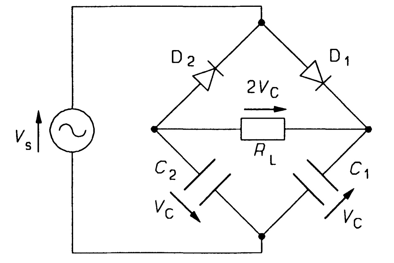
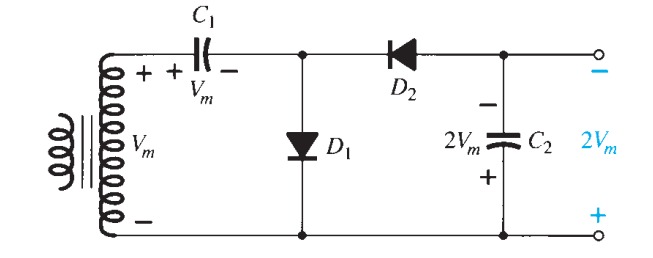
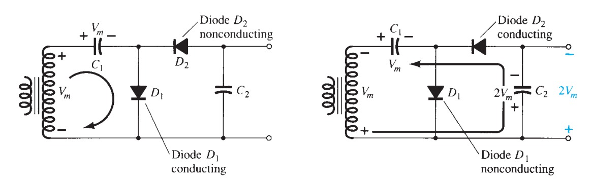
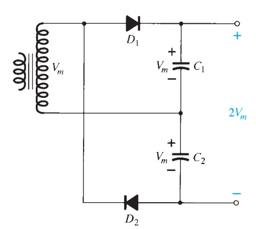
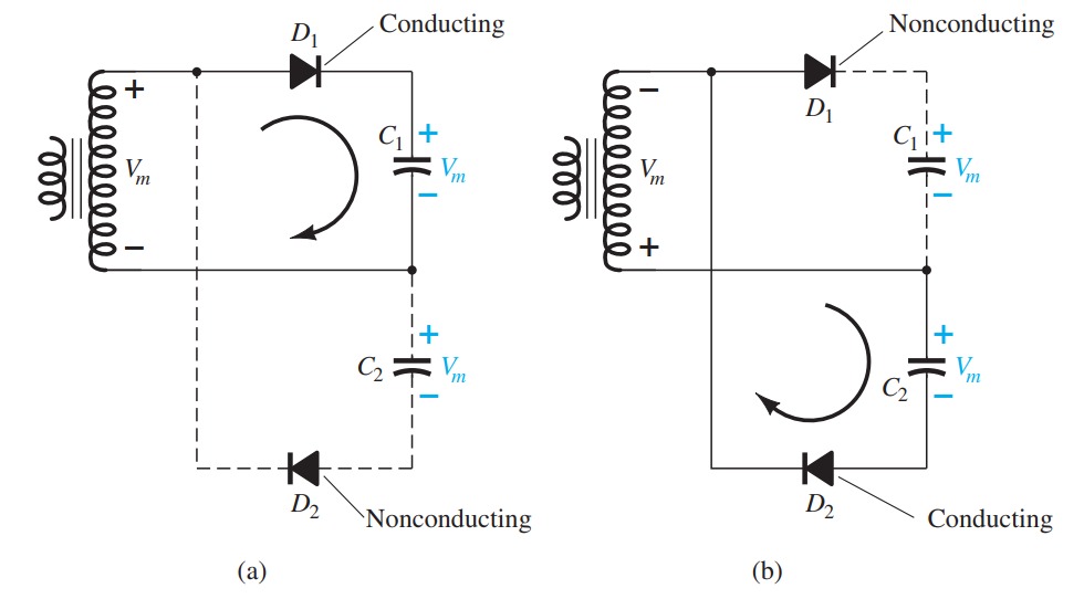
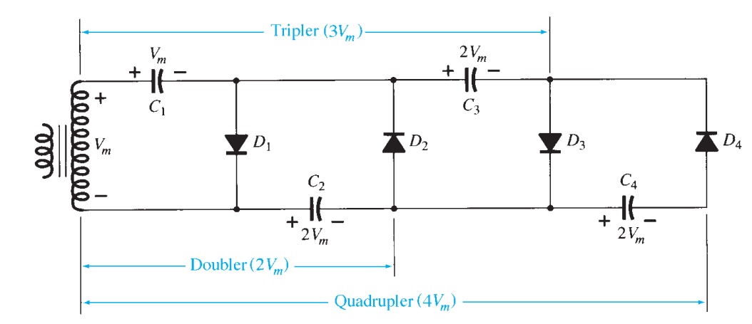
The circuit most often met is the full-wave voltage doubler of figure 24, and is the same as the full-wave bridge rectifier with diodes \(D_{2}\) and \(D_{3}\) replaced by capacitors. In this circuit the maximum voltage from the supply, \(V_{P}\), is doubled (but for the forward drop of two diodes). On the positive cycle \(D_{1}\) conducts and \(C_{}1\) charges up to \(V_{P}- 0.6\) volts. On the negative half-cycle \(D_{2}\) conducts and charges \(C_{2}\) up to \(V_{P} - 0.6\) volts, so the maximum output voltage is \(2 V_{P} - 1.2\) volts, with the usual ripple.
Logarithmic conversion
Since the current through a diode is an exponential function of the voltage across it, we can take the logarithm of a signal fairly easily with the circuit shown in figure 25a. If the signal is smaller than 0.6 V, then compensation for diode drop such as that shown in figure 25b is necessary.
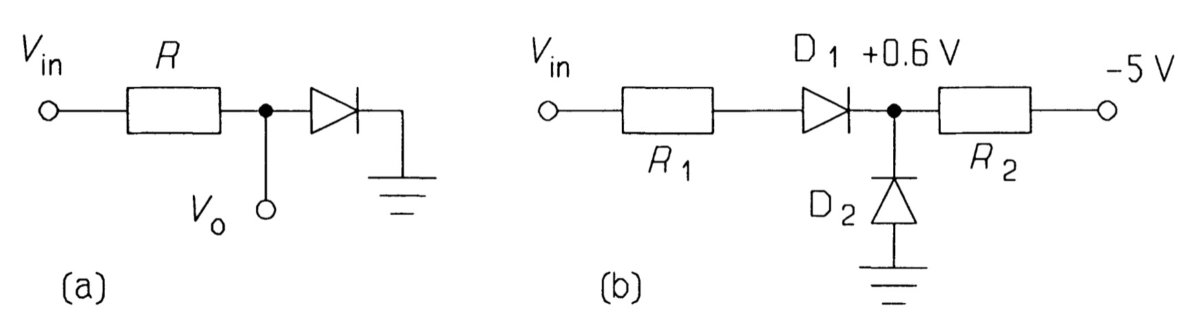
In this circuit, unless \(R_{2} \leq\leq R_{1}\), \(D_{2}\) will not pass enough current to keep its cathode at \(0.6\) \(V\). The circuit will not work well over large input voltage ranges. Logarithmic converters are available as ICs which use operational amplifiers with a \(p-n\) junction in the feedback loop to give an output that is the logarithm of the input voltage. By suitable compensation these can be made to perform well over several voltage decades.
Model Questions
- A small silicon diode obeys the rectifier equation, \(I= Is[exp(qV/\eta kT- 1]\), with \(\eta = 1.8\). If the forward current is \(5\) \(mA\) at \(300\) \(K\) when the forward voltage is \(0.7\) \(V\), what is \(I_{s}\)? If the temperature of the junction increases to \(350\) \(K\), what will the forward voltage be if the current remains \(5\) \(mA\)? [\(I_{s}= 1.485\) \(nA\), \(V = 0.63\) \(V\)]
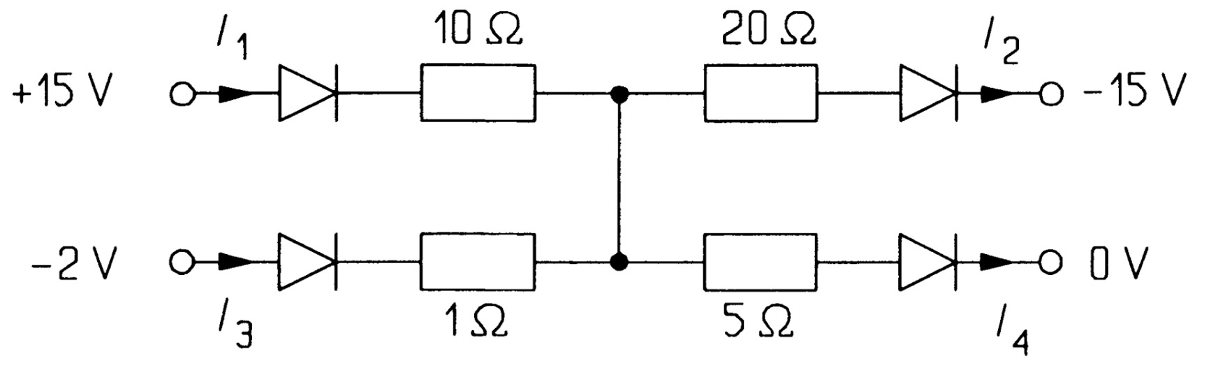
- The diodes in the circuit of figure \(PN2\) have negligible resistance and forward voltage drops of \(1\) \(V\). Find \(I_{1}\), \(I_{2}\), \(I_{3}\) and \(I_{4}\) [\(I_{1} = 1.143\) \(A\), \(I_{2} = 0.829\) \(A\), \(I_{}3 = 0\), \(I_{4} = 0.314\) \(A\)]
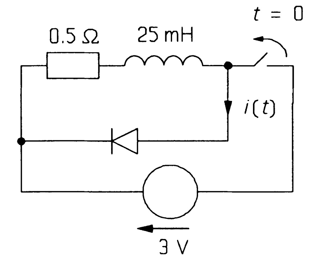
- In the circuit of figure \(PN3\), steady-state conditions obtain prior to the switch opening. Find \(i(t)\) if the diode has negligible resistance and a forward voltage drop of \(0.7\) \(V\). When is \(i(t) = 0\)? What is the power consumption as a function of time? What is the average power consumption during discharge? [\(i(t) = (25 - 2t)u(t) + 2(t- 12.5)u(t- 12.5)\) \(A\), \(t = 12.5\) \(s\), \(p(t) = (17.5 - 1.4t)u(t) - 1.4(t- 12.5)u(t- 12.5)\) \(W\), \(8.75\) \(W\)]
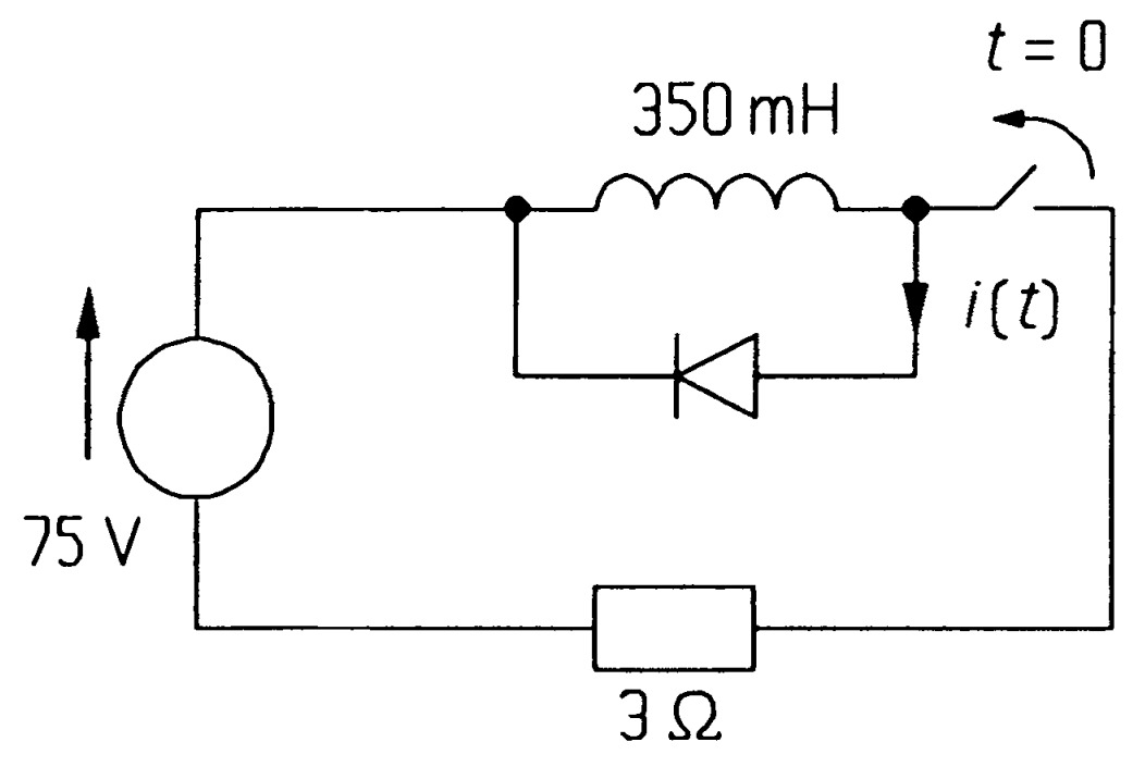
- In the circuit of figure \(PN4\) the switch was closed for a long time before being opened at \(t = 0\). If the diode's forward drop is \(1\) \(V\), what is \(i(t)\)? When is the current zero? [\(i(t) = -2 + 8 exp( -Rt/L)\) \(A\) (\(for 0 \leq t \leq t_{0}\)). \(i(t) = 0\) when \(t = t_{0} = 69.3\) \(ms\)]
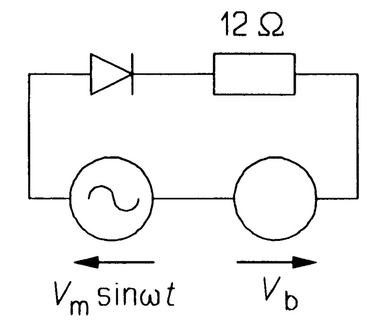
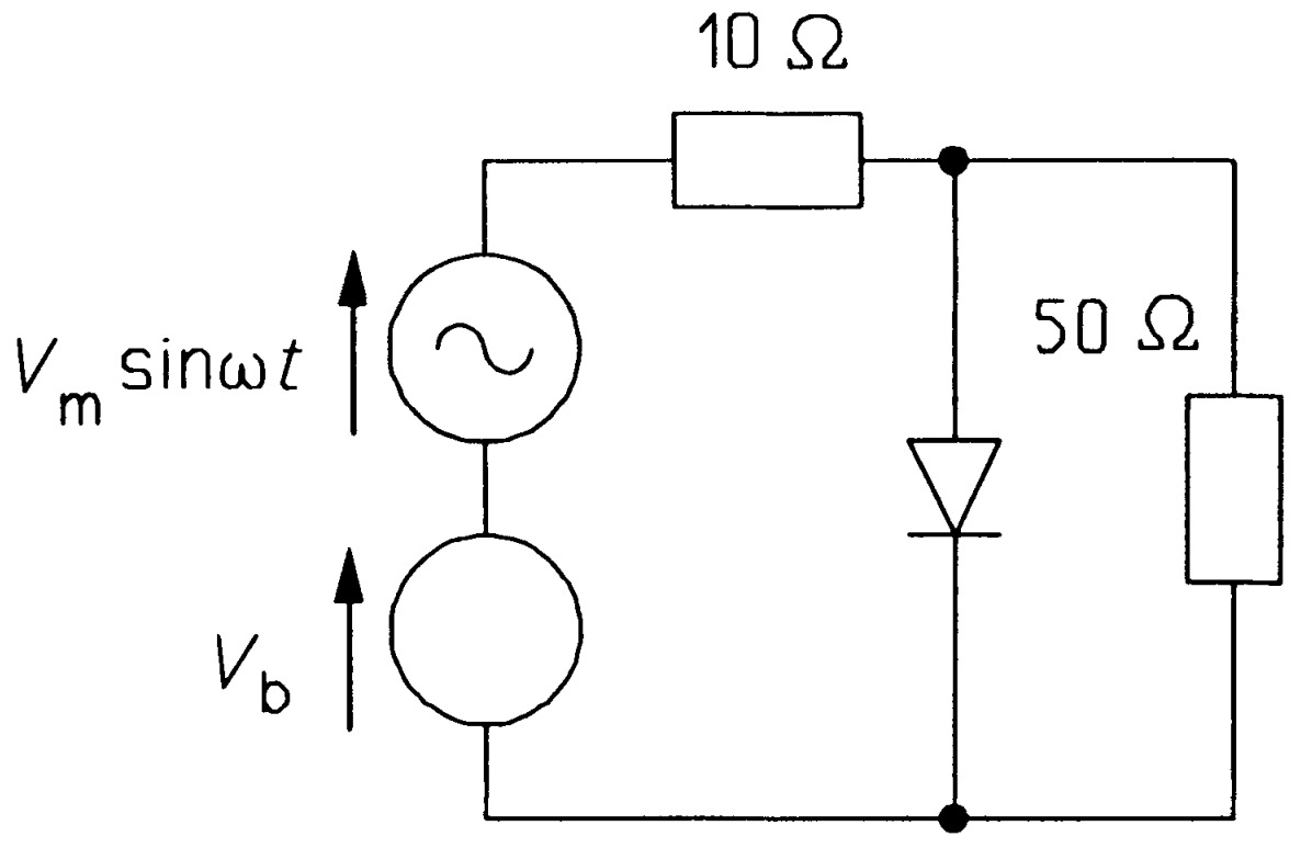
- In the circuit of figure \(PN5\), the diode's forward voltage drop is \(0.7\) \(V\). What is the average power developed in the load if \(V_{m} = 6\) \(V\) and \(V_{b}\) is (a) \(1\) \(V\) (b) \(2\) \(V\) and (c) \(4\) \(V\)? [(a) \(322\) \(mW\) (b) \(165\) \(mW\) (c) \(15.9\) \(mW\)]
- Repeat problem 5 with \(V_{b}\) reversed. [(a) \(0.842\) \(W\) (b) \(1.097\) \(W\) (c) \(1.400\) \(W\)]
- In the circuit of figure \(PN7\) the diode has a dynamic resistance of \(0.9\) \(\Omega\) at all currents and a forward voltage drop of \(0.6\) \(V\) at very low current. If \(V_{m}\)\( = 0.2\) \(V\) and \(V_{b} = 1.2\) \(V\), what are the diode current and voltage? [ \(18 sin \omega t + 43.3\) \(mA\), \(0.0162 sin \omega t + 0.639\) \(V\)]
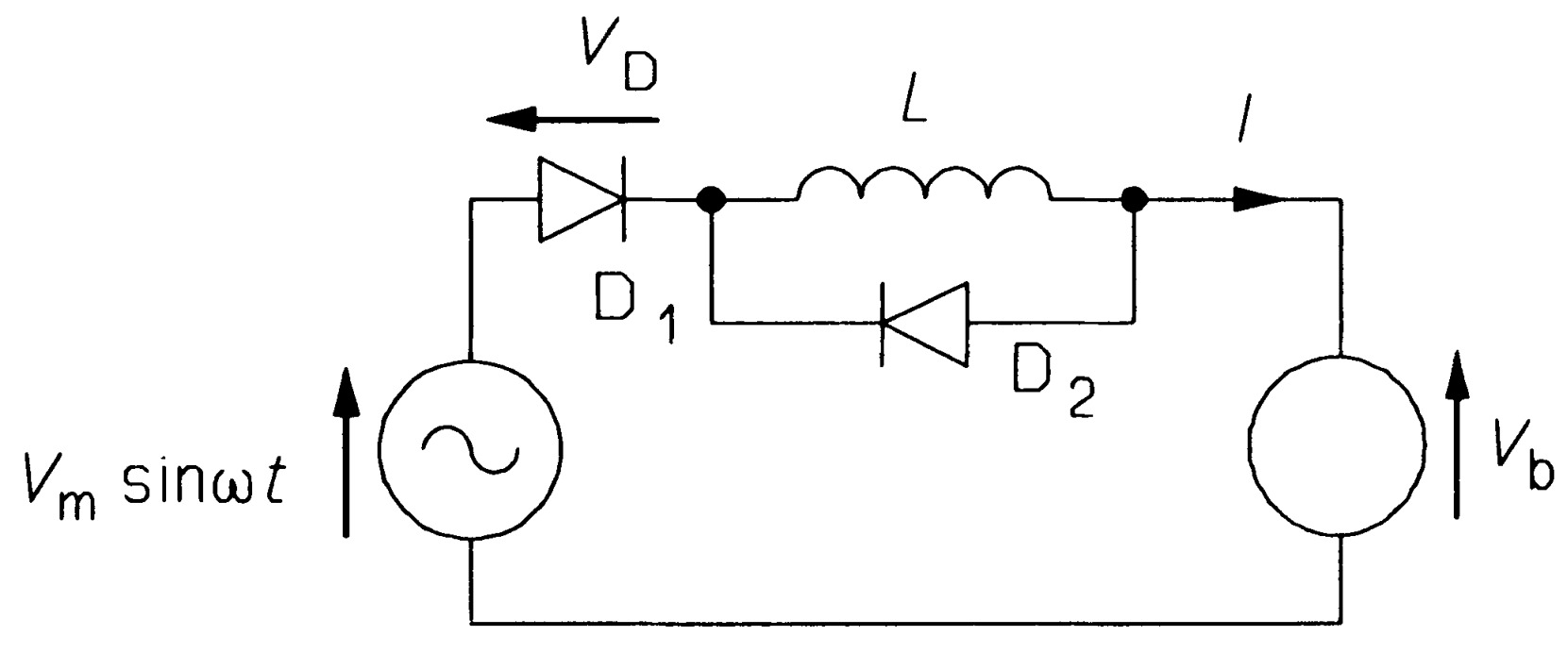
- For the circuit of figure \(PN8\) show that \(I_{max}= [2V_{m}cos\theta_{c} + (V_{b} + V_{D} )(2\theta_{c}- \pi)]/\omega L\), where \(\theta_{c}\), the conduction angle, is \(sin^{-1} [(V_{D} + V_{b})/V_{m}]\). What is \(I_{max}\) if \(V_{m} = 10\) \(V\), \(V_{b} = 5\) V, \(V_{D} = 0.7\) \(V\), \(L = 15\) \(mH\) and \(f= 50\) \(Hz\)? What is \(V_{b}\) if \(I_{max}= 0.5\) \(A\)? [\(I_{max} = 1.154\) \(A\), \(V_{b} = 6.82\) \(V\)]
- A varactor diode is used in a tuned circuit that gives an output frequency of \(1/2\pi\sqrt{(LC)}\), where \(C\) is the diode capacitance given by \(C = 100/\sqrt{V}\) \(pF\). \(V\) is the reverse bias voltage of the diode and can be varied from \(1\) \(V\) to \(20\) \(V\). What is the frequency range of the tuned circuit if \(L = 10\) \(pH\)? Derive an expression for the relative change of frequency with voltage. Calculate from this the change in frequency produced by a \(1 \%\) change in diode voltage at \(7\) \(MHz\). [\(5\) \(MHz\) to \(10.6\) \(MHz\), \(17.5\) \(kHz\)]
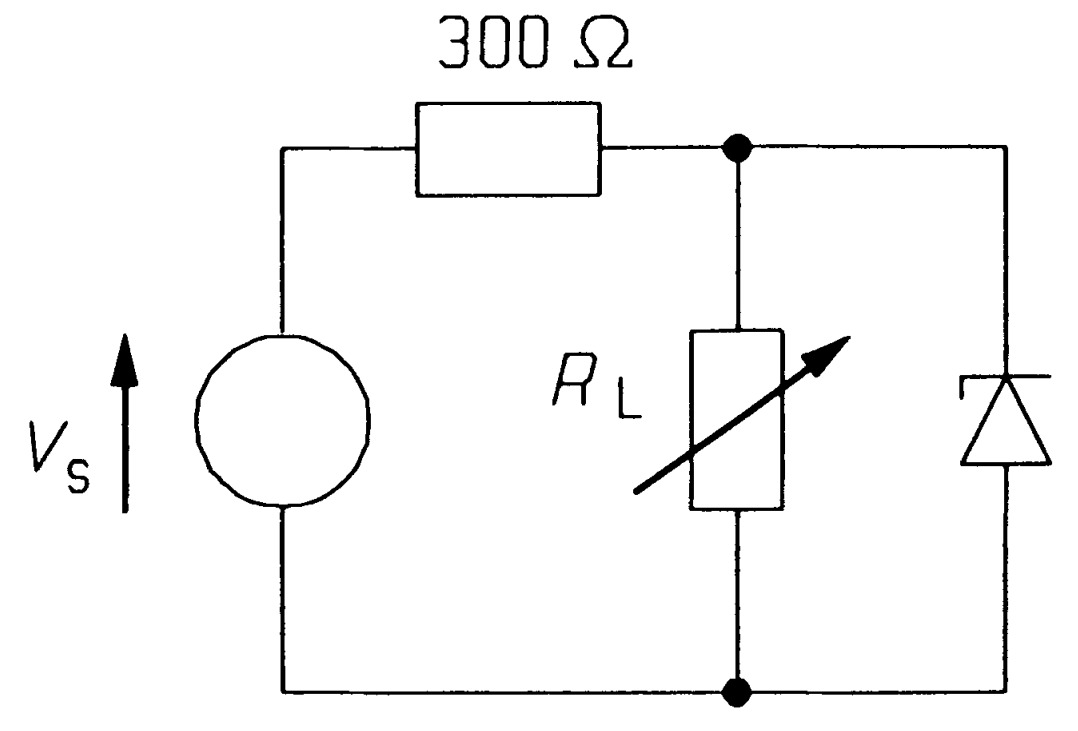
- For the circuit of figure \(PN10\) the zener voltage is \(10\) \(V\) at a current of \(10\) \(mA\). If the dynamic resistance of the diode is \(15\) \(\Omega\), calculate the maximum and minimum load voltages if the load current can vary from \(5\) \(mA\) to \(25\) \(mA\) (independent of the supply voltage) and the supply voltage from \(20\) to \(25\) \(V\) (independently from the load current). What is the minimum power rating required for the zener? [\(10.5\) \(V\), \(9.976\) \(V\). \(455\) \(mW\), but at least 500 mW is needed to give a safety margin]
- The energy of a photon is given approximately by \(E= 1.24/\lambda\), where \(E\) is in \(eV\) and the wavelength, \(\lambda\), is in \(pm\). If the range of photon energies in eV is \(3k_{B}T\), show that the linewidth is given by \(\Delta\lambda = 2.4k_{B}T\lambda^{2}\). What is the \(Q (= \lambda/\Delta\lambda)\) of a GaAs LED at \(77\) \(K\) (the boiling point of liquid nitrogen) and at \(300\) \(K\) given that its bandgap is \(1.42\) \(eV\)? (The \(Q\) of a LED indicates how sharp the spectral line is.) [\(Q\) \(= 73\) and \(Q = 19\)]