Transistors
Introduction
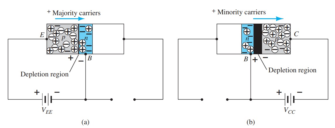
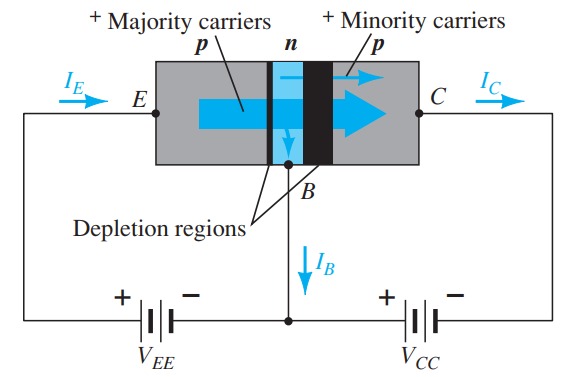
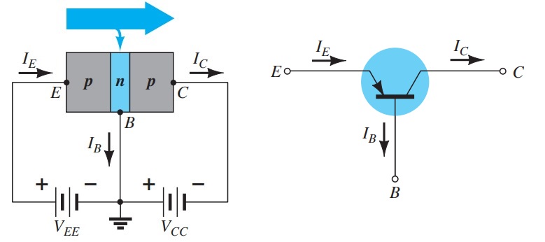
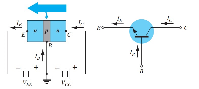
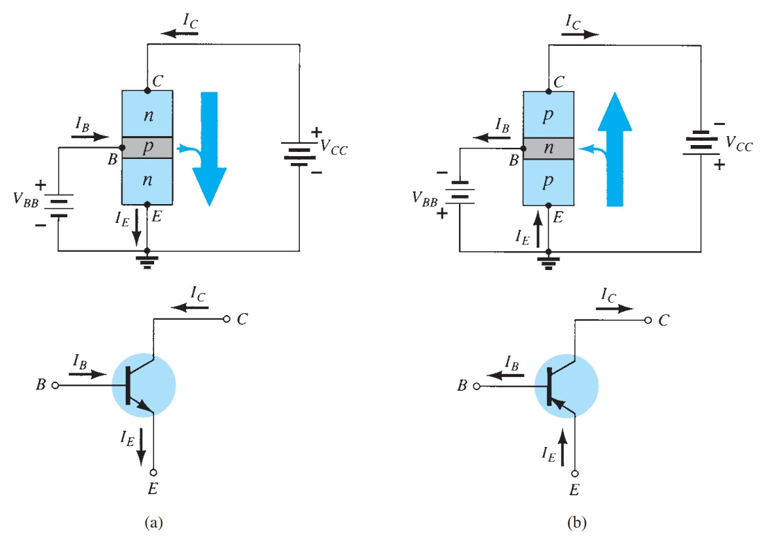
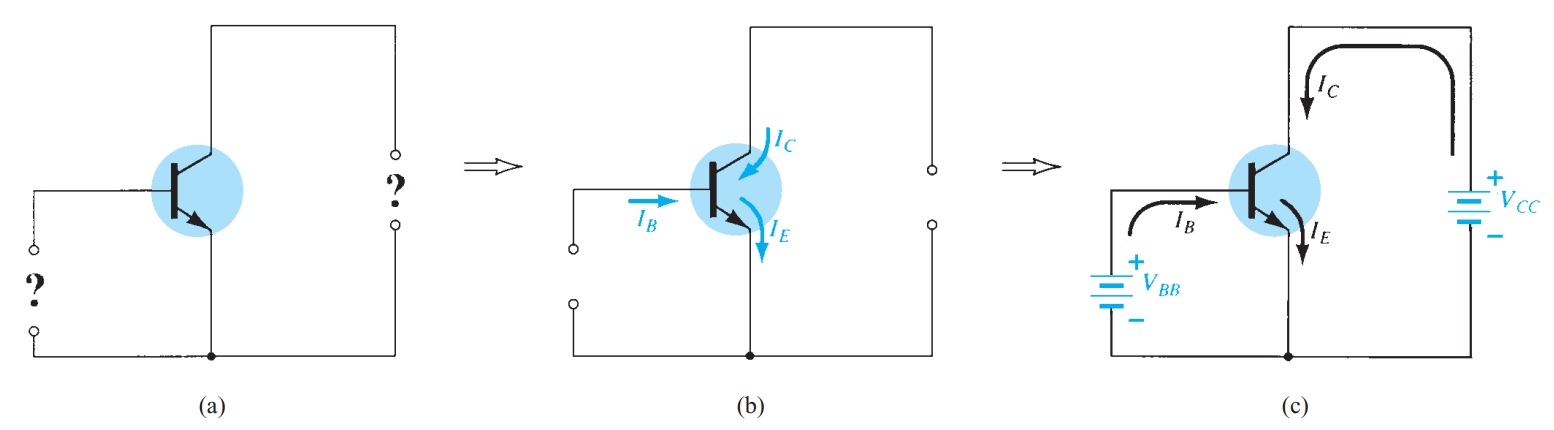
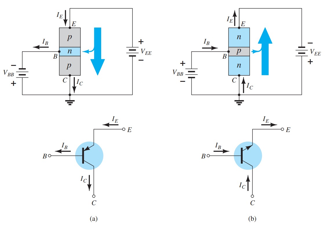
The transistor is a three-layer semiconductor device consisting of either two n - and one p -type layers of material or two p - and one n -type layers of material. The former is called an npn transistor , and the latter is called a pnp transistor .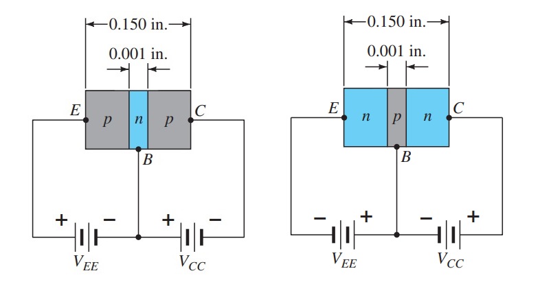
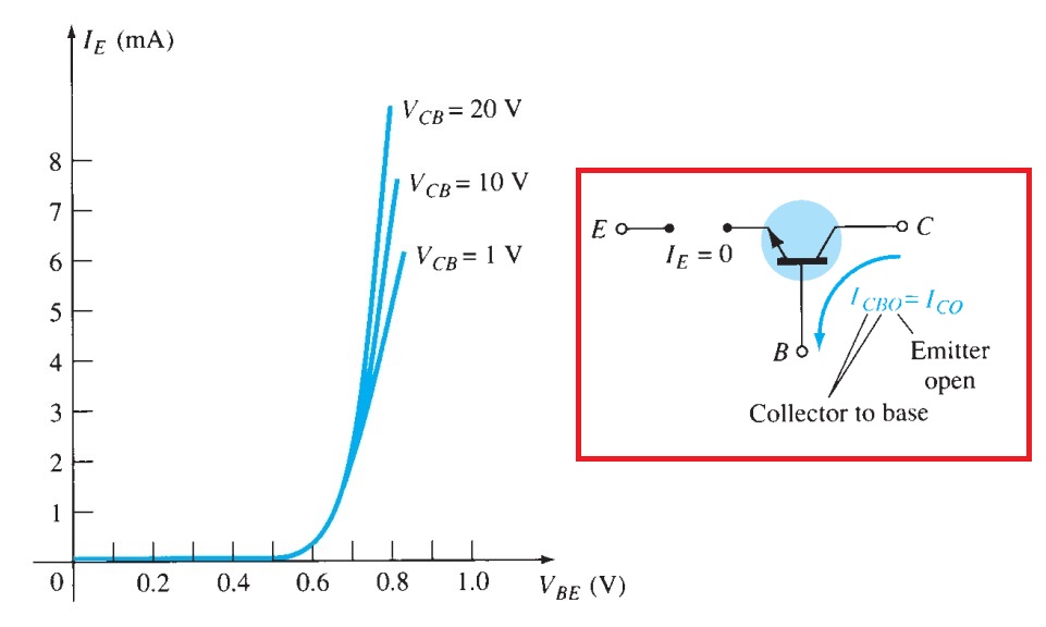
Common-Base Configuration
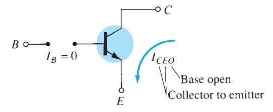
Common-Emitter Configuration
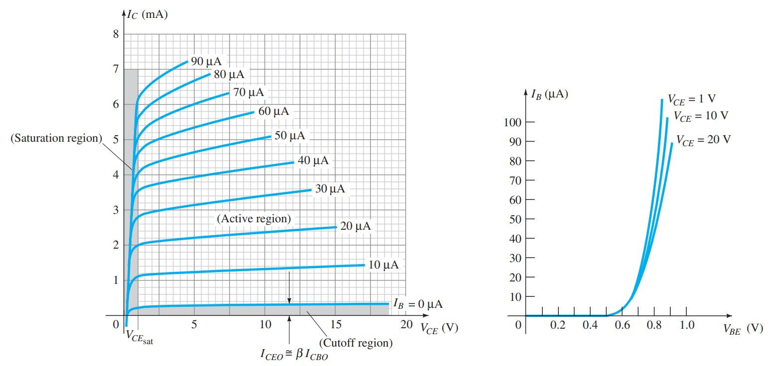
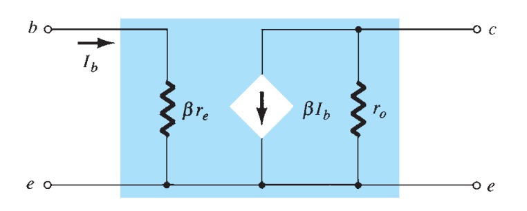
Beta \(\beta\)
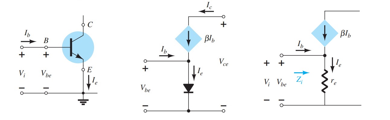
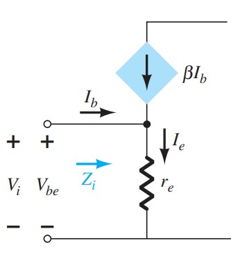
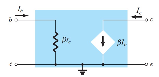
In the dc mode the levels of I C and I B are related by a quantity called beta and defined by the following equation: \[ \beta_{dc}=\frac{I_{C}}{I_{B}} \] For ac situations an ac beta is defined as follows: \[ \beta_{ac}=\frac{\Delta I_{C}}{\Delta I_{B}} \] \[ I_{E}= I_{C}+I_{B} \] \[ \frac{I_{C}}{\alpha}= I_{C}+\frac{I_{C}}{\beta} \] or \[ \frac{1}{\alpha}= 1+\frac{1}{\beta} \] or \[ \alpha = \frac{\beta}{\beta +1} \] or \[ \beta = \frac{\alpha}{1-\alpha} \] Additionally, \[ I_{CEO}=\frac{I_{CBO}}{(1-\alpha)} \] but, \[ \frac{1}{1-\alpha} = \beta + 1 \] or \[ I_{CEO}=(\beta + 1)~I_{CBO} \] or \[ I_{CEO}=\beta I_{CBO} \] and \[ I_{C}=\beta I_{B} \] also, \[ I_{E}=I_{C}+I_{B} = \beta I_{B}+I_{B} \] or \[ I_{E}=(\beta + 1)I_{B} \]Common-Collector Configuration
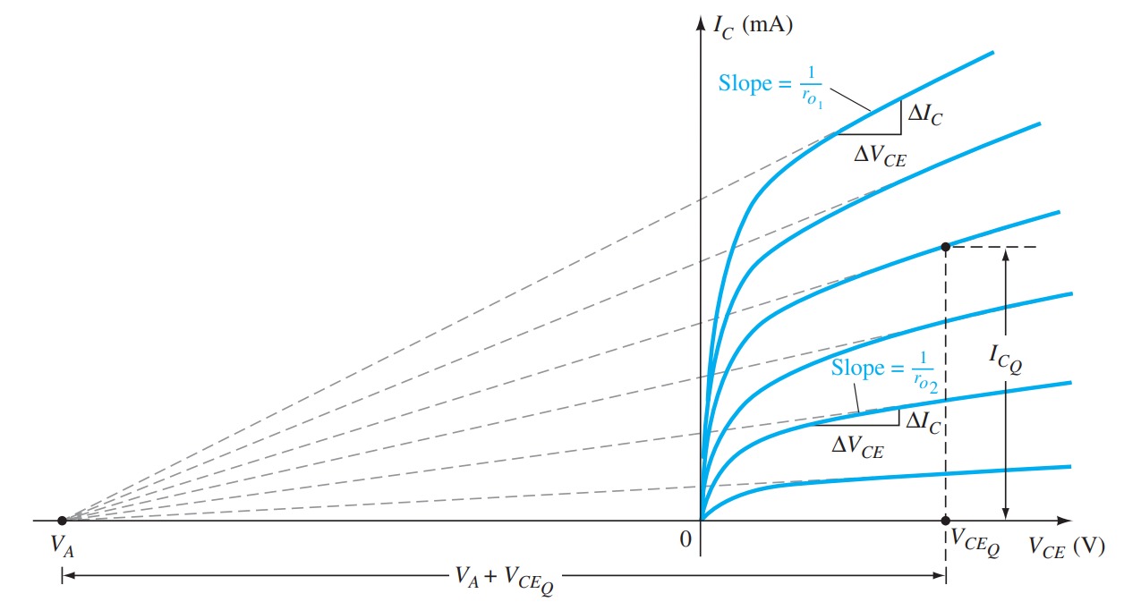
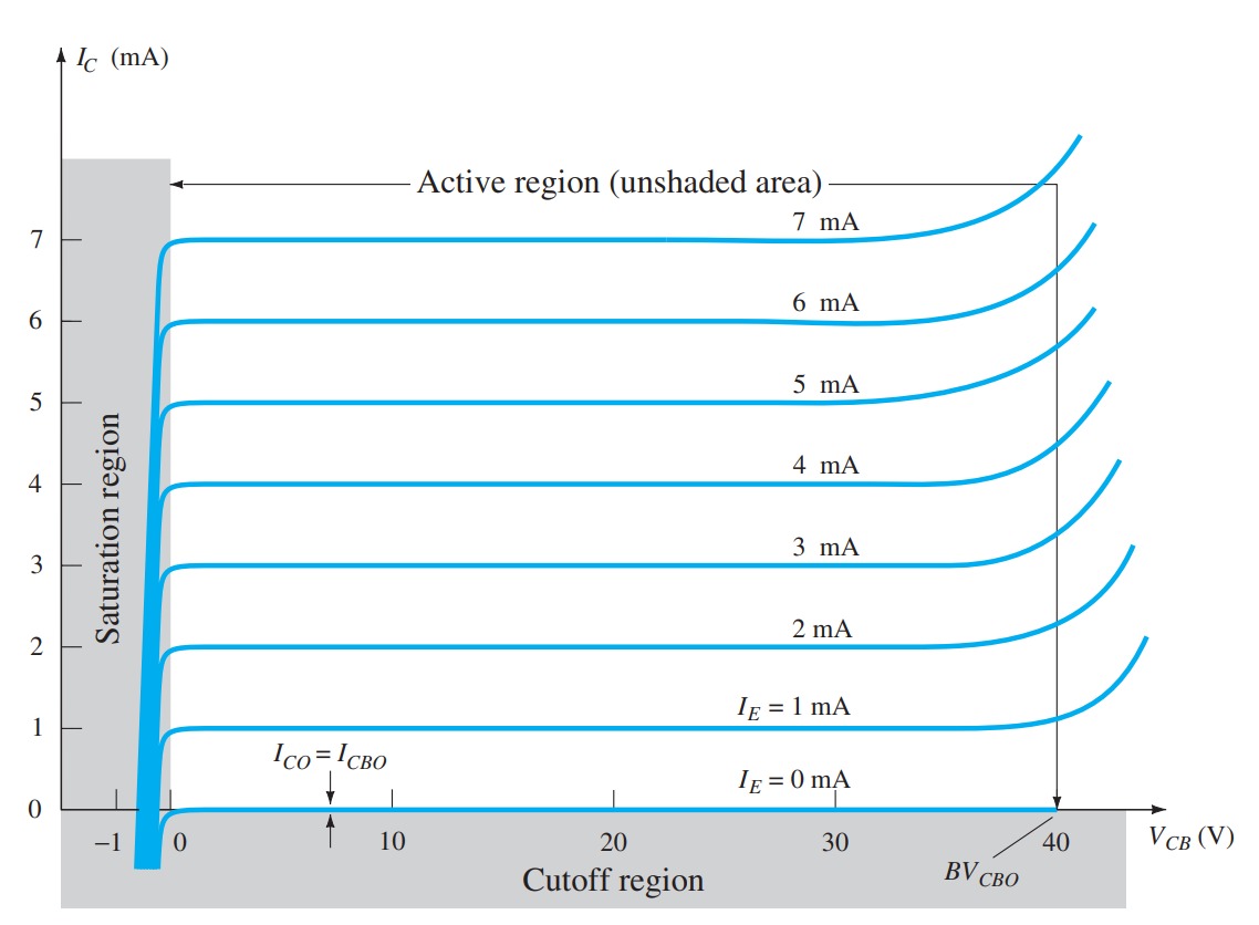
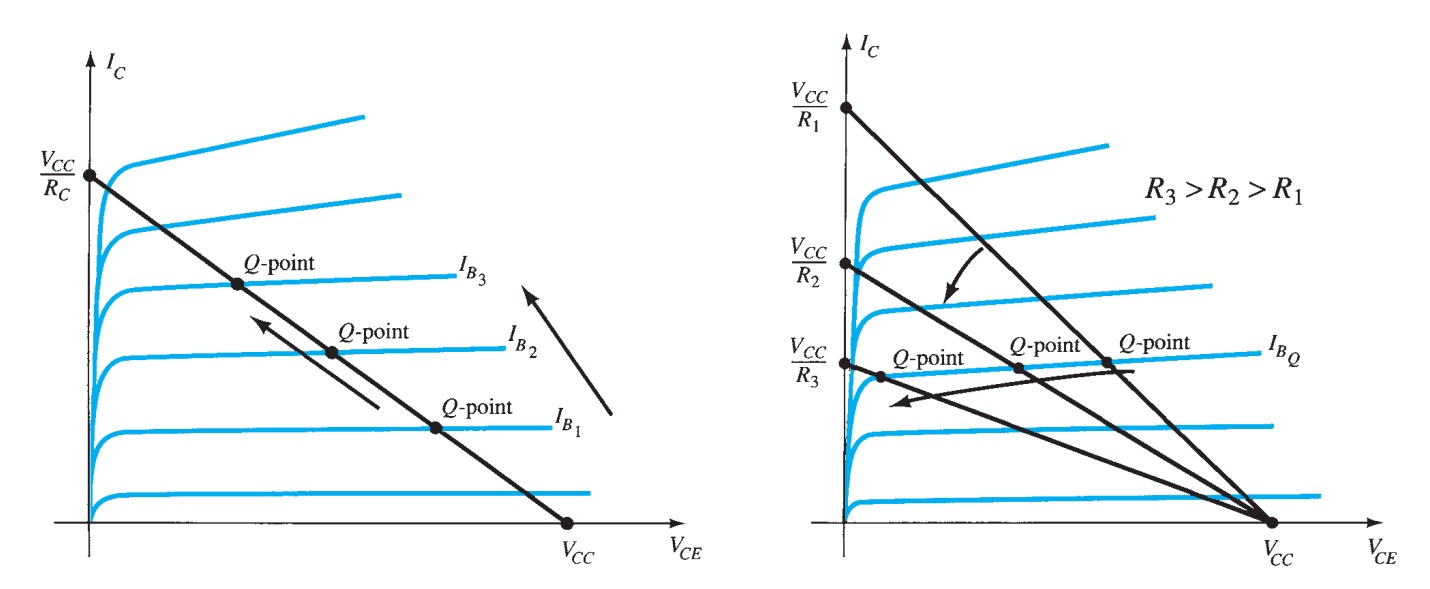
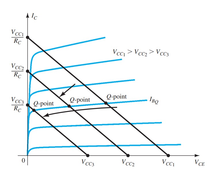
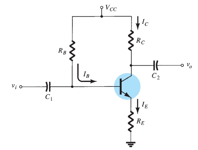
Limits of Operation
For each transistor there is a region of operation on the characteristics that will ensure that the maximum ratings are not being exceeded and the output signal exhibits minimum distortion.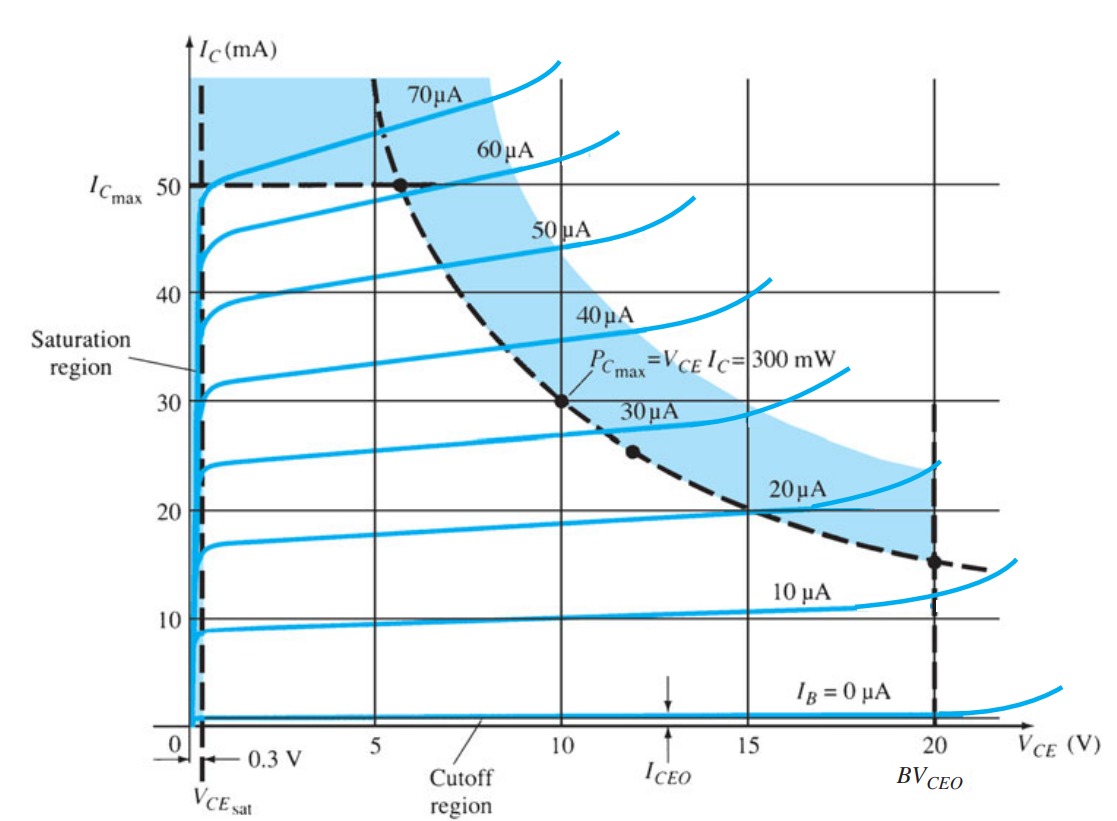
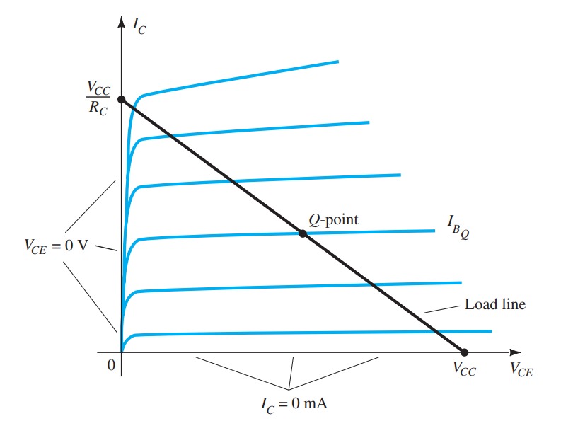
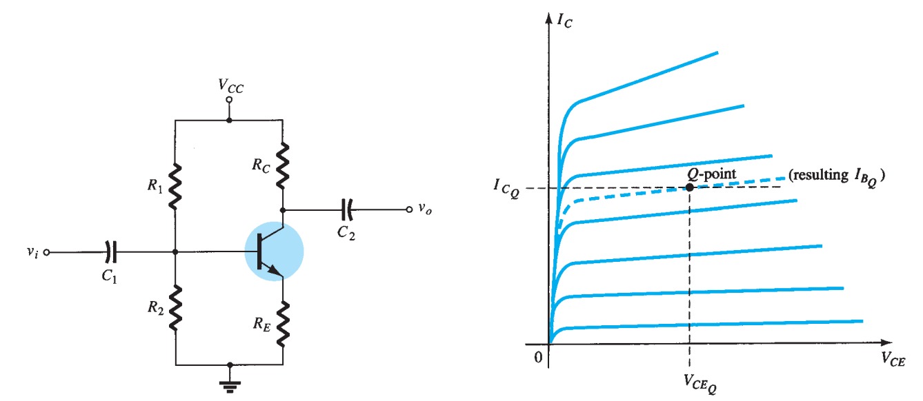
Operating point
1. The base–emitter junction must be forward-biased (p-region voltage more positive), with a resulting forward-bias voltage of about 0.6 V to 0.7 V. 2. The base–collector junction must be reverse-biased (n-region more positive), with the reverse-bias voltage being any value within the maximum limits of the device. Operation in the cutoff, saturation, and linear regions of the BJT characteristic are provided as follows: 1. Linear-region operation: Base–emitter junction forward-biased Base–collector junction reverse-biased 2. Cutoff-region operation: Base–emitter junction reverse-biased Base–collector junction reverse-biased 3. Saturation-region operation: Base–emitter junction forward-biased Base–collector junction forward-biased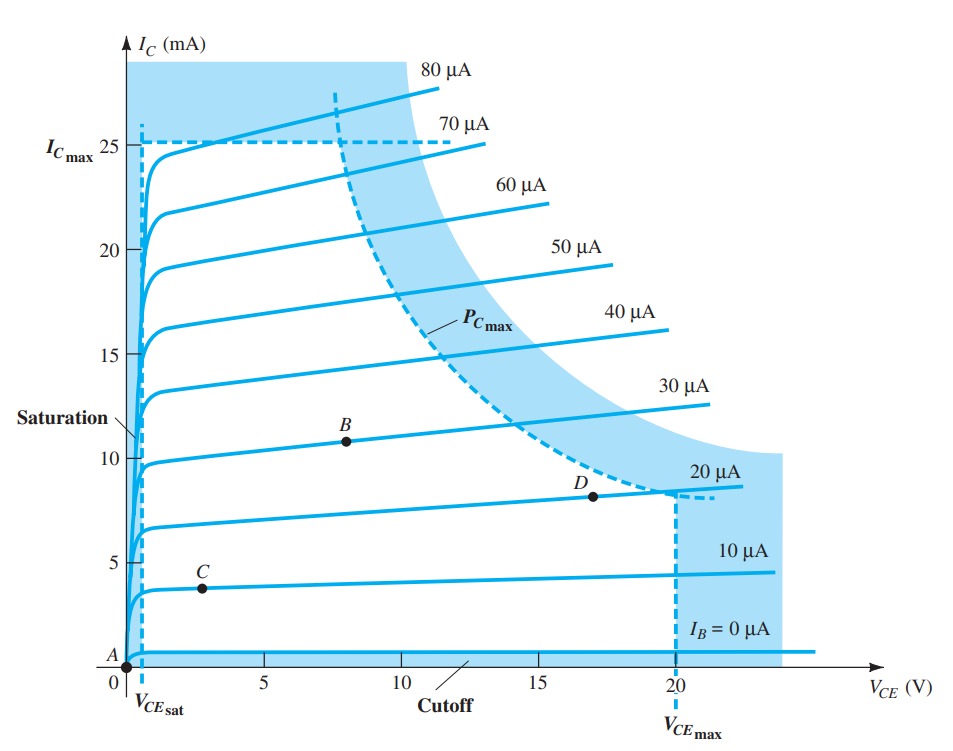
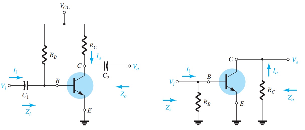
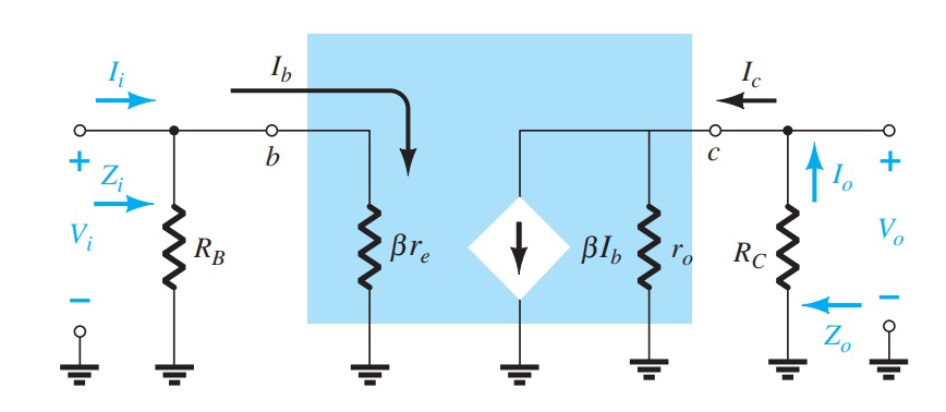
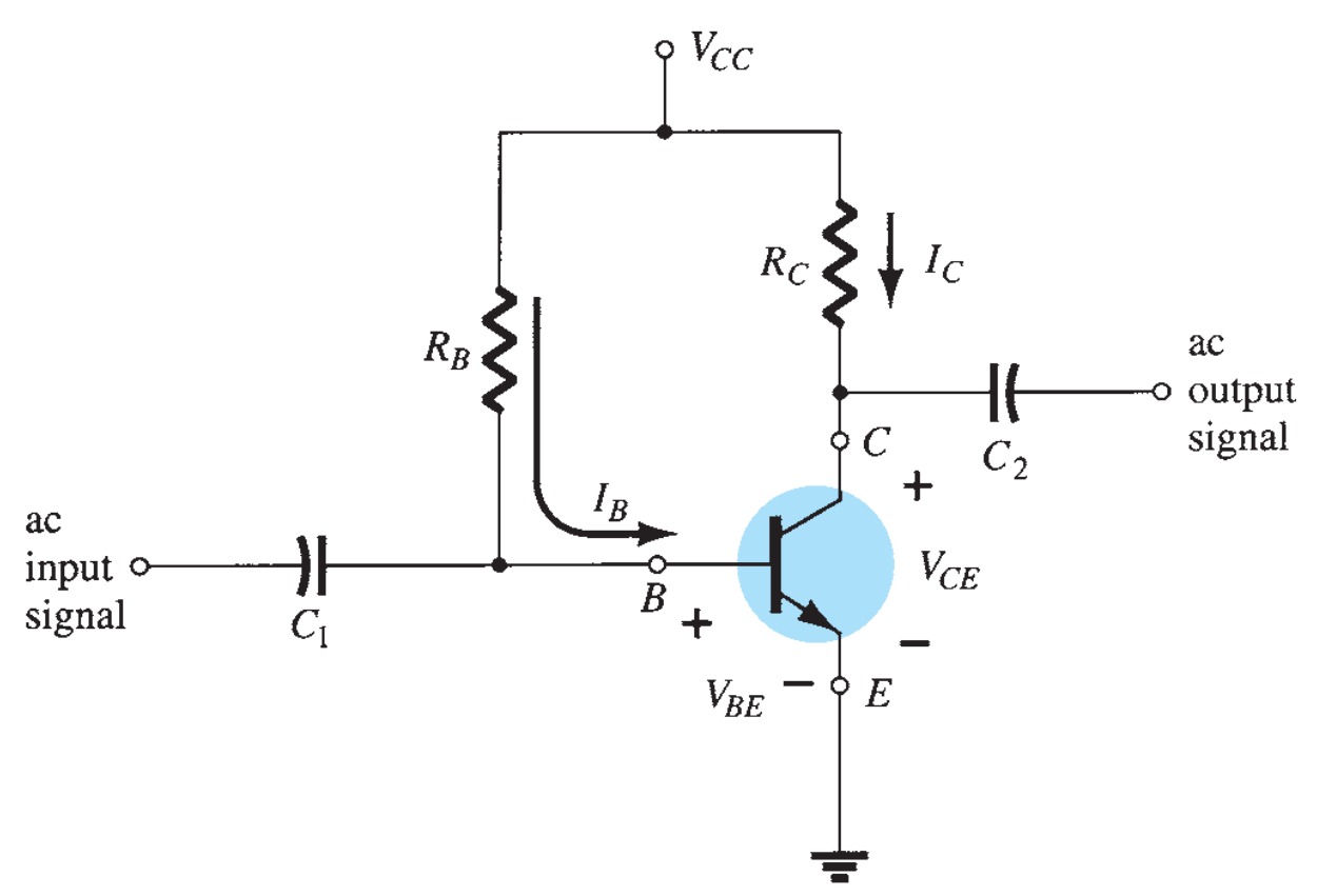
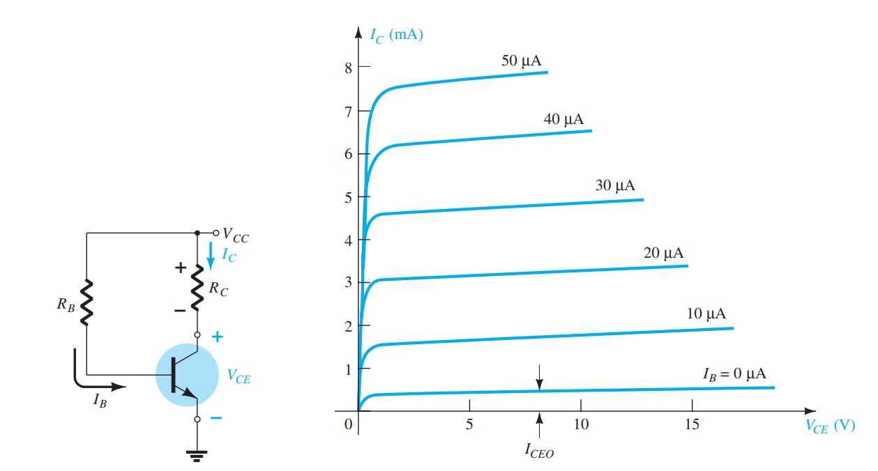
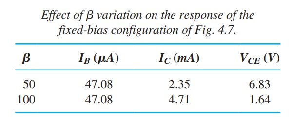
Fixed-Bias Configuration
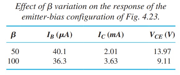
Emitter-Bias Configuration
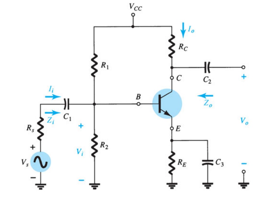
Voltage Divider bised Configuration
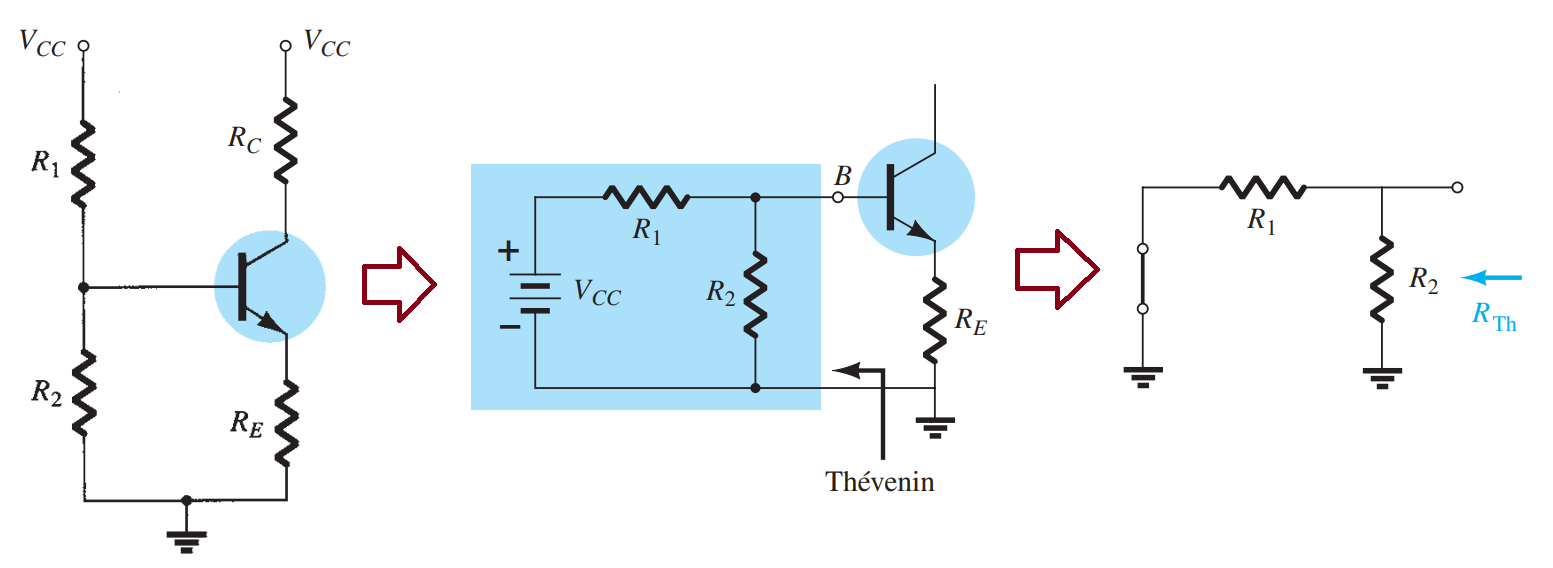
Exact Analysis
The Thévenin equivalent network for the network to the left of the base terminal can then be found in the following manner:
Thévenin Resistance \(R_{Th}\) The voltage source is replaced by a short-circuit equivalent as
\[R_{Th} = R_{1} || R_{2}\] Thévenin voltage \(E_{Th}\) The voltage source \(V_{CC}\) is returned to the network and the open-circuit Thévenin voltage determined as follows:
Applying the voltage-divider rule gives \[ E_{Th} = V_{R_{2}} = \frac{R_{2}V_{CC}}{(R_{1} + R_{2})}\]
The Thévenin network is then redrawn and \(I_{BQ}\) can be determined by first applying Kirchhoff's voltage law in the clockwise direction for the loop indicated:
\[E_{Th} - I_{B}R_{Th} - V_{BE} - I_{E}R_{E} = 0 \]
Substituting \(I_{E} = (\beta + 1)I_{B}\) and solving for \(I B\) yields
\[I_{B} = \frac{(E_{Th} - V_{BE})}{(R_{Th} + (\beta + 1)R_{E})}\]
Although initially appears to be different from those developed earlier, note that the numerator is again a difference of two voltage levels and the denominator is the base resistance plus the emitter resistor reflected by \((\beta + 1)\).
Once \(I_{B}\) is known, the remaining quantities of the network can be found in the same manner as developed for the emitter-bias configuration. That is,
\[ V_{CE} = V_{CC} - I_{C}(R_{C} + R_{E})\]
The remaining equations for \(V_{E}\), \(V_{C}\), and \(V_{ B}\) are also the same as those obtained for the emitter-bias configuration.
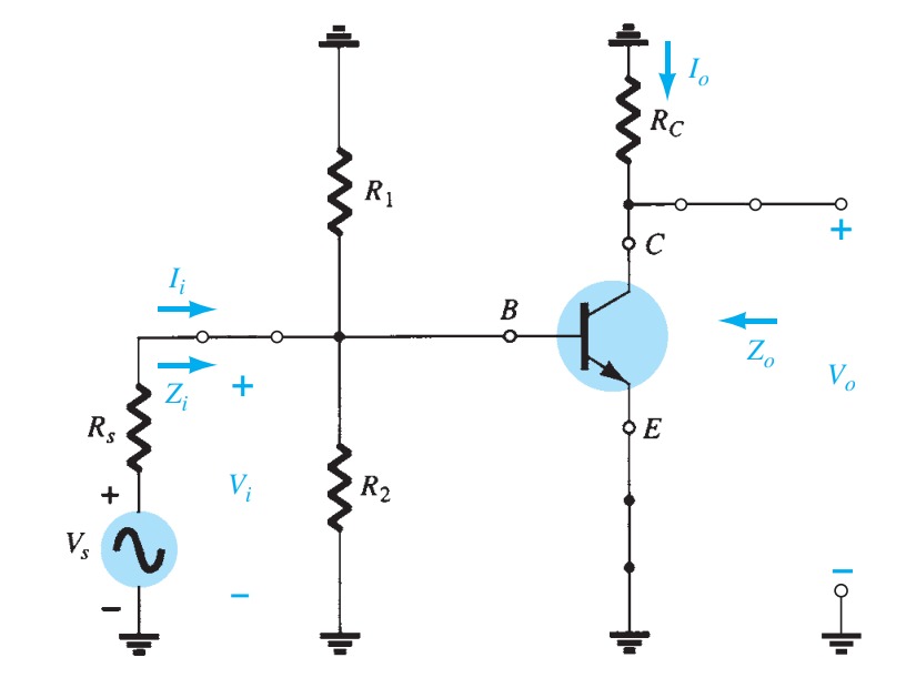
Approximate Analysis
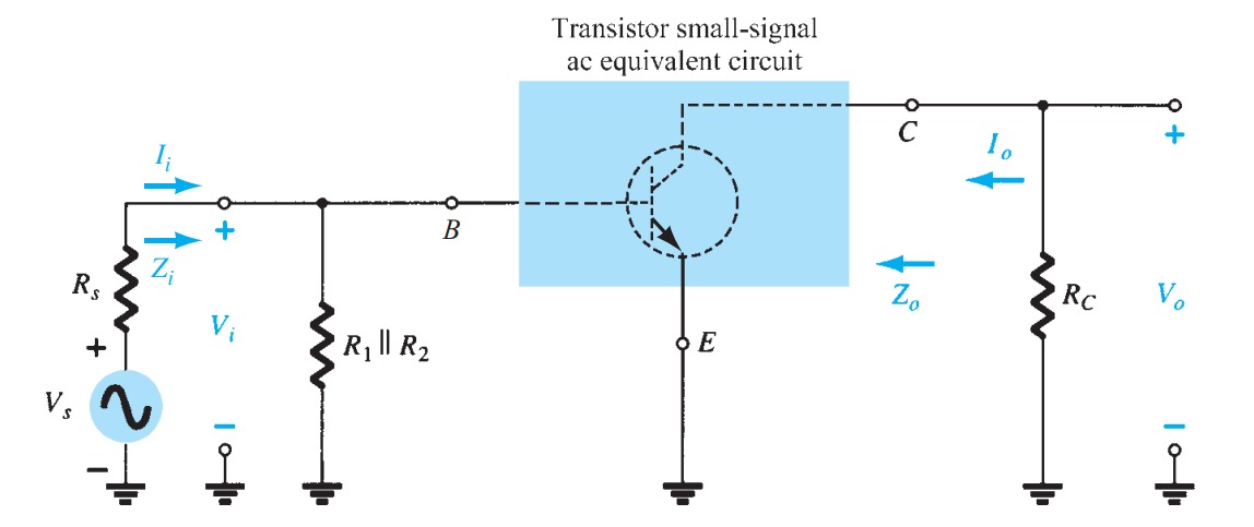
The input section of the voltage-divider configuration can be represented by the network. The resistance \(R_{i}\) is the equivalent resistance between base and ground for the transistor with an emitter resistor \(R_{E}\).
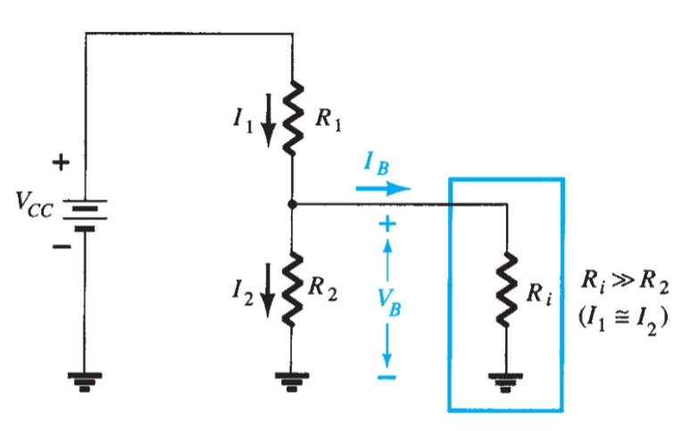
The emitter resistor, which is part of the collector–emitter loop, “appears as” \((\beta + 1)R_{E}\) in the base–emitter loop.
\[R_{i}= (\beta + 1)R_{E}\]
If \(R_{i}\) is much larger than the resistance \(R_{2}\) , the current \(I_{B}\) will be much smaller than \(I_{2}\) (current always seeks the path of least resistance) and \(I_{2}\) will be approximately equal to \(I_{1}\). If we accept the approximation that \(I_{B}\) is essentially \(0\) \(A\) compared to \(I_{1}\) or \(I_{2}\) , then \(I_{1} = I_{2}\), and \(R_{1}\) and \(R_{2}\) can be considered series elements. The voltage across \(R_{2}\) , which is actually the base voltage, can be determined using the voltage-divider rule. That is,
\[V_{B} = \frac{R_{2}V_{CC}}{(R_{1} + R_{2})}\]
Because \(R_{i} = (\beta + 1)R_{E} \cong \beta R_{E}\) the condition that will define whether the approximate approach can be applied is
\[\beta R_{E} \geq 10R_{2}\] In other words, if \(\beta\) times the value of \(R_{E}\) is at least 10 times the value of \(R_{2}\), the approximate approach can be applied with a high degree of accuracy.
Once \(V_{B}\) is determined, the level of \(V_{E}\) can be calculated from
\[V_{E} = V_{B} - V_{BE}\] and the emitter current can be determined from \[I_{E} = \frac{V_{E}}{R_{E}}\]
and \[I_{CQ} \cong I_{E}\]
The collector-to-emitter voltage is determined by \[V_{CE} = V_{CC} - I_{C}R_{C} - I_{E}R_{E}\]
but because \(IE \cong IC\),
\[V_{CEQ} = V_{CC} - I_{C}(R_{C} + R_{E})\]
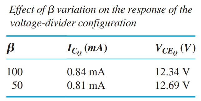
In the sequence of calculations \(\beta\) does not appear and \(I_{B}\) was not calculated. The \(Q\)-point (as determined by \(I_{CQ}\) and \(V_{CEQ}\)) is therefore independent of the value of \(beta\).
Emitter Follower Configuration
Emitter follower configuration is where the output is taken off the emitter terminal as shown in figure. The configuration is not the only one where the output can be taken off the emitter terminal. In fact, any of the configurations just described can be used so long as there is a resistor in the emitter leg.
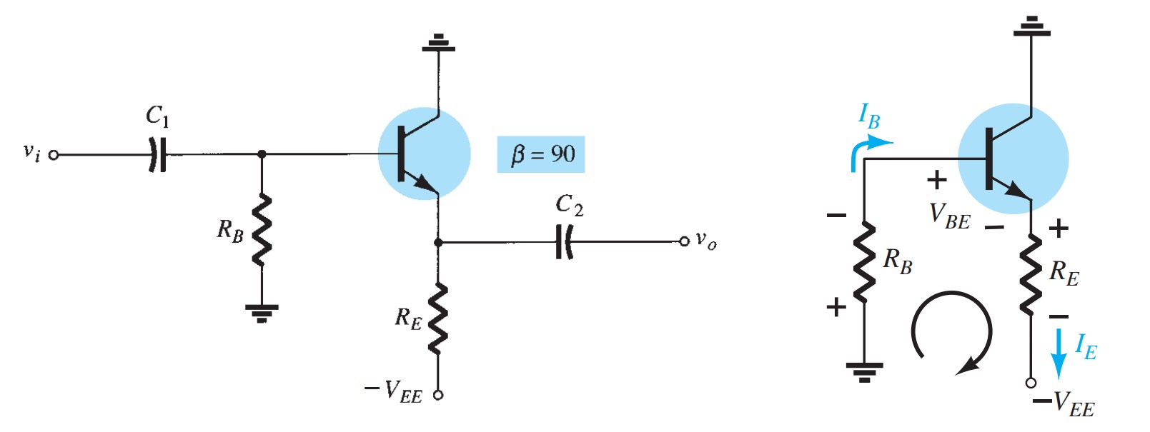
Applying Kirchhoff's voltage rule to the input circuit will result in
\[-I_{B}R_{B} - V_{BE} - I_{E}R_{E} + V_{EE} = 0 \]
and using \(I_{E} = (\beta + 1)I_{B}\)
\[I_{B}R_{B} + (\beta + 1)I_{B}R_{E} = V_{EE} - V_{BE}\]
so that
\[I_{B} = \frac{V_{EE} - V_{BE}}{R_{B} + (\beta + 1)R_{E}}\]
For the output network, an application of Kirchhoff's voltage law will result in
\[-V_{CE} - I_{E}R_{E} + V_{EE} = 0 \]
and
\[V_{CE} = V_{EE} - I_{E}R_{E}\]
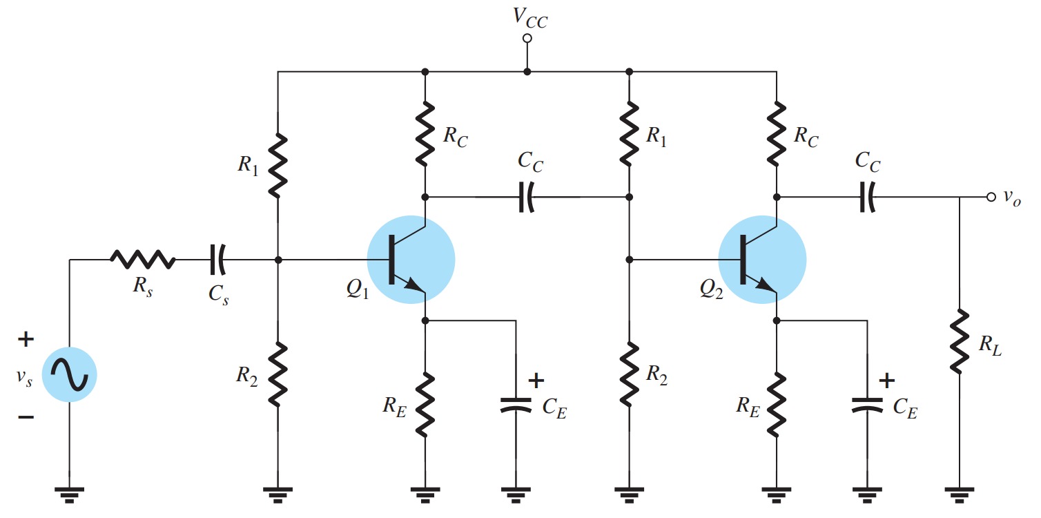
R-C Coupled BJT amplifier
The collector output of one stage is fed directly into the base of the next stage using a coupling capacitor \(C_{C}\). The capacitor is chosen to ensure that it will block dc between the stages and act like a short circuit to any ac signal. The network has two voltage-divider stages, but the same \(RC\) coupling can be used between any combination of networks such as the fixed-bias or emitter-follower configurations. Substituting an open-circuit equivalent for \(C_{C}\) and the other capacitors of the network will result in the two bias arrangements. The methods of analysis introduced in this chapter can then be applied to each stage separately since one stage will not affect the other.
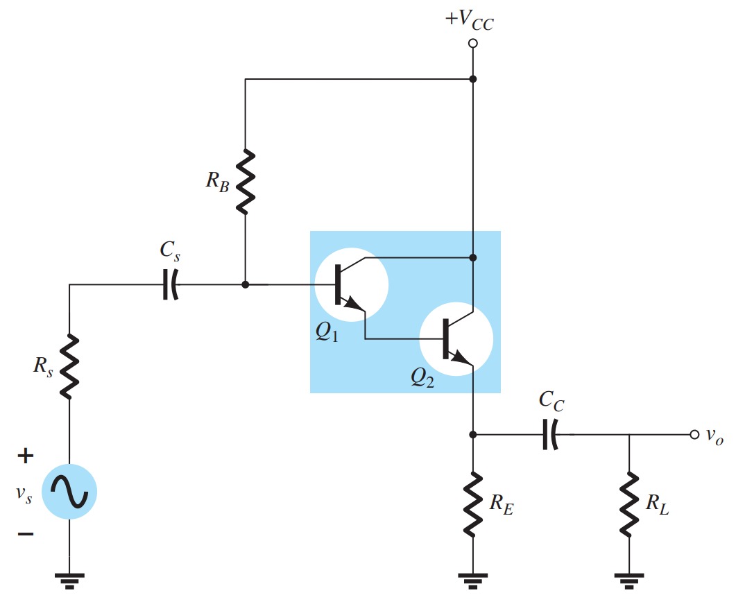
Darlington Pair
The Darlington configuration feeds the output of one stage directly into the input of the succeeding stage. Since the output is taken directly off the emitter terminal, you will find in the next chapter that the ac gain is very close to 1 but the input impedance is very high, making it attractive for use in amplifiers operating off sources that have a relatively high internal resistance. If a load resistor were added to the collector leg and the output taken off the collector terminal, the configuration would provide a very high gain.
Transistor Switching Network
The application of transistors is not limited solely to the amplification of signals. Through proper design, transistors can be used as switches for computer and control applications. The network can be employed as an inverter in computer logic circuitry. Note that the output voltage \(V_{C}\) is opposite to that applied to the base or input terminal. In addition, note the absence of a dc supply connected to the base circuit. The only dc source is connected to the collector or output side, and for computer applications is typically equal to the magnitude of the “high” side of the applied signal—in this case 5 V. The resistor \(R_{B}\) will ensure that the full applied voltage of \(5\) \(V\) will not appear across the base-to-emitter junction. It will also set the \(I_{ B}\) level for the “on” condition. Proper design for the inversion process requires that the operating point switch from cutoff to saturation along the load line.
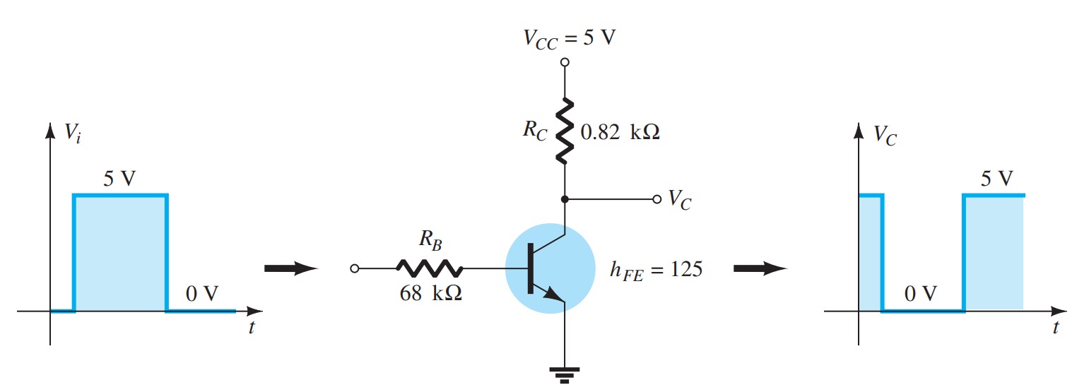
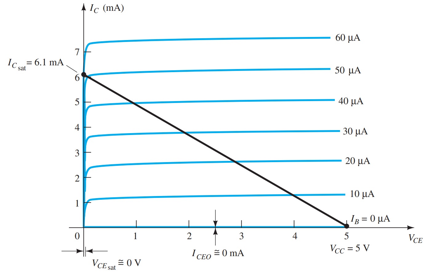
In Fig this requires that \(I_{B} \cong 50\) \(mA\). The saturation level for the collector current for the circuit of Fig. is defined by
\[I_{C_{sat}} = {V_{CC}}{R_{C}}\]
The level of \(I_{B}\) in the active region just before saturation results can be approximated by the following equation:
\[I_{B_{max}} \cong {I_{C_{sat}}} {b_{dc}}\]
For the saturation level we must therefore ensure that the following condition is satisfied:
\[I_{B} \gt \frac{I_{C_{sat}}}{b_{dc}}\]
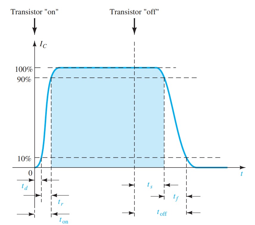
There are transistors that are referred to as switching transistors due to the speed with which they can switch from one voltage level to the other. In Fig the periods of time defined as \(t_s\), \(t_d\), \(t_r\), and \(t_f\) are provided versus collector current. Their impact on the speed of response of the collector output is defined by the collector current response. The total time required for the transistor to switch from the “off” to the “on” state is designated as ton and is defined by
\[t_{\text{on}} = t_r + t_d\]
with \(t_d\) the delay time between the changing state of the input and the beginning of a response at the output. The time element \(t_r\) is the rise time from 10% to 90% of the final value.
The total time required for a transistor to switch from the “on” to the “off” state is referred to as \(t_{\text{off}}\) and is defined by
\[t_{\text{off}} = t_s + t_f \]
where \(t_s\) is the storage time and \(t_f\) the fall time from 90% to 10% of the initial value.
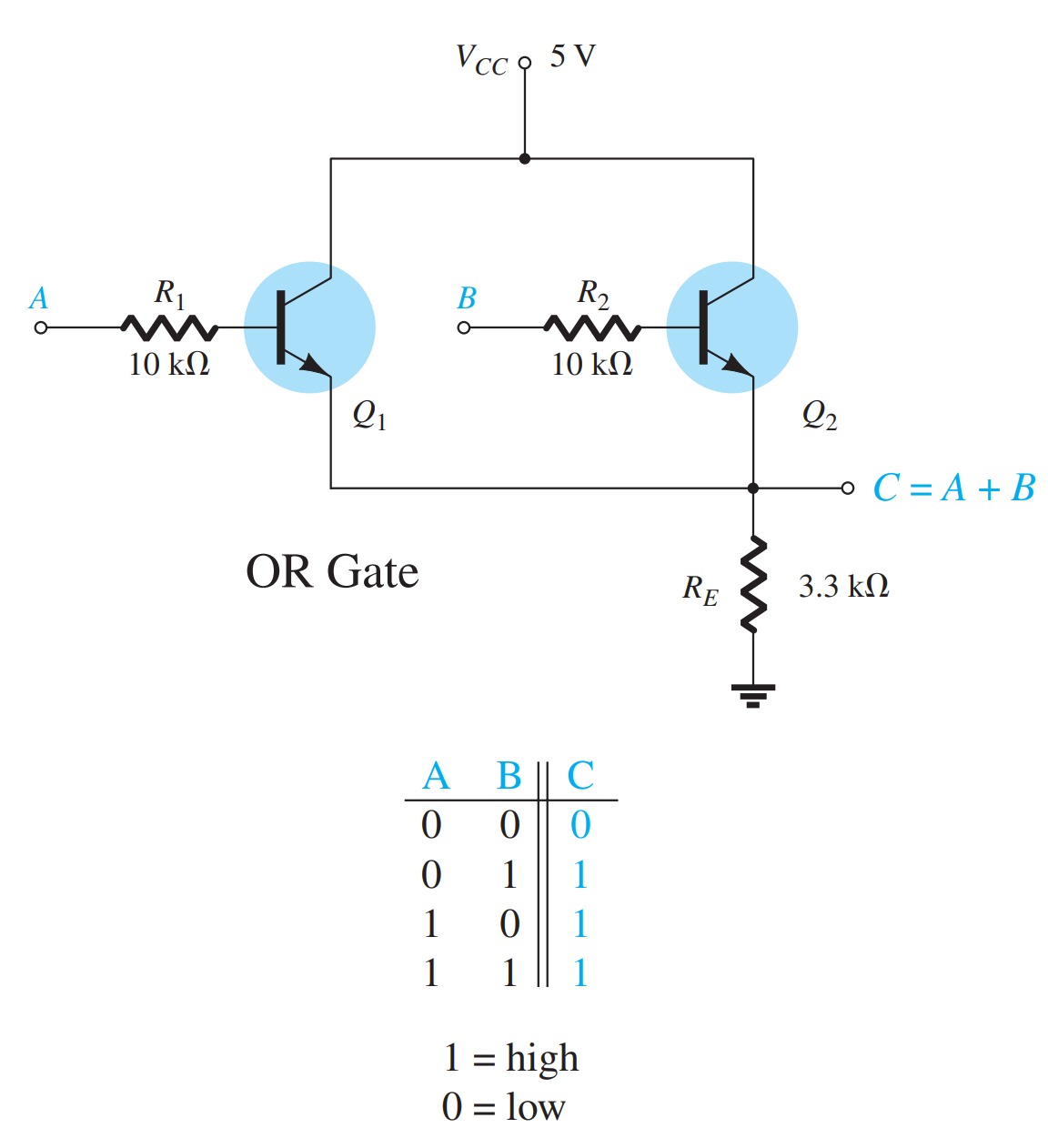
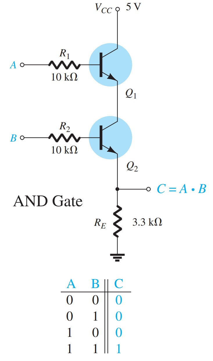
Logic gates
Bias Stability
The stability of a system is a measure of the sensitivity of a network to variations in its parameters. In any amplifier employing a transistor the collector current \(I_{C}\) is sensitive to each of the following parameters:
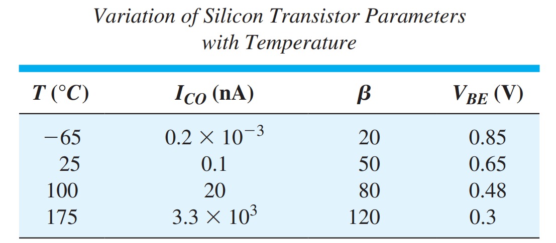
- \(\beta\): increases with increase in temperature
- \(V_{BE}\): decreases about \(2.5\) \(mV\) per degree Celsius (\(°C\)) increase in temperature
- \(I_{CO}\) (reverse saturation current): doubles in value for every \(10\) \(°C\) increase in temperature
Stability Factors \(S(I_{CO})\), \(S (V_{BE})\), and \(S(\beta)\)
A stability factor \(S\) is defined for each of the parameters affecting bias stability as follows:
\[S(I_{CO}) = \frac{\delta I_{C}}{\delta I_{CO}}\]
\[S(V_{BE}) = \frac{\delta I_{C}}{\delta V_{BE}}\]
\[S(\beta) = \frac{\delta I_{C}}{\delta \beta}\]
- Networks that are quite stable and relatively insensitive to temperature variations have low stability factors.
- The higher the stability factor, the more sensitive is the network to variations in that parameter.
AC Analysis - BJT