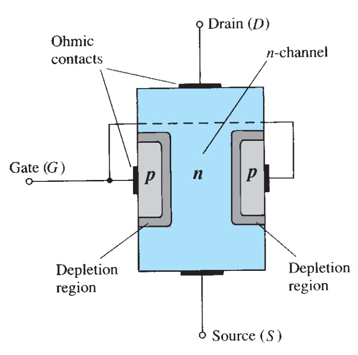
Fig showing the schematic diagram of n-channel JFET
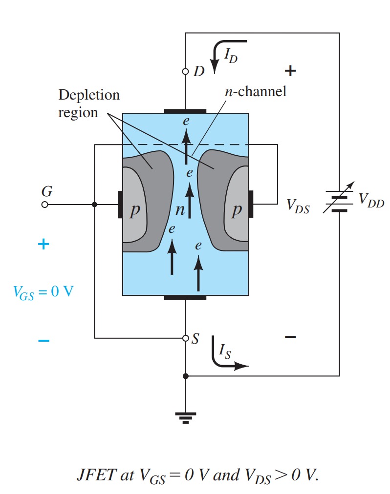
Fig showing the voltage biasing of JFET
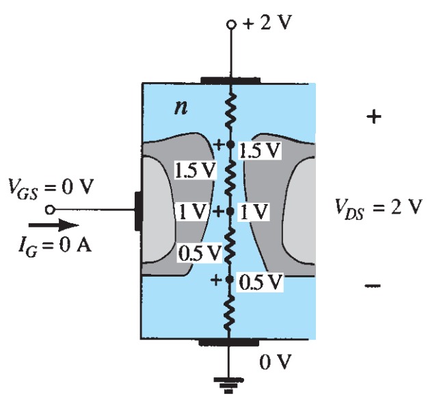
Fig showing the voltage division along the n-channel of the JFET
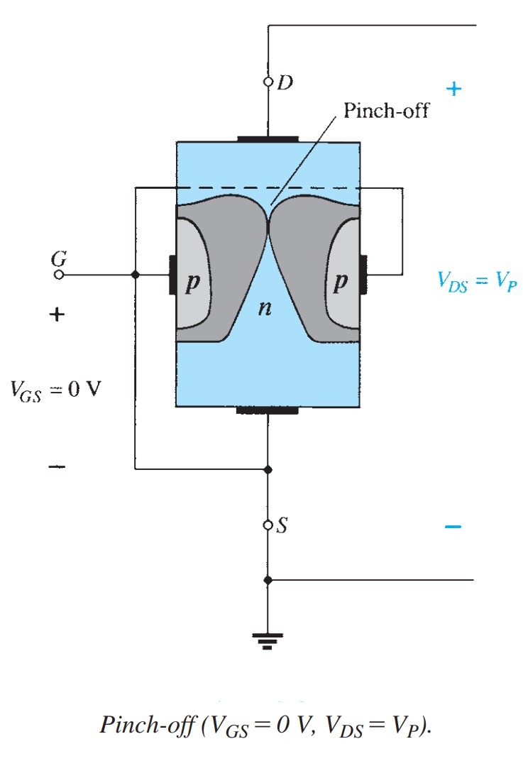
Fig showing the Pinch off condition of a JFET
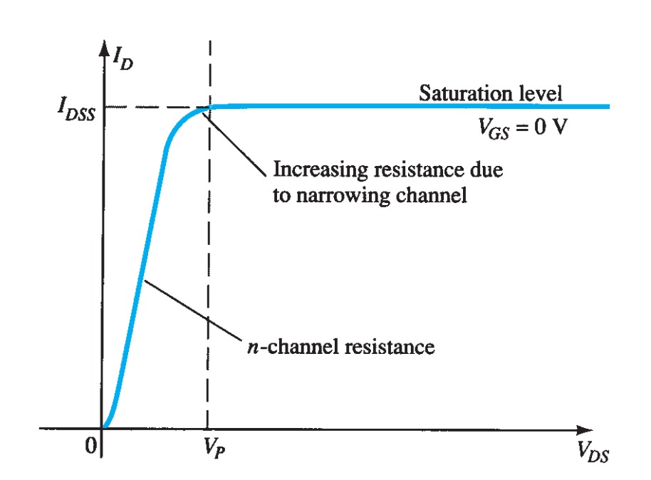
Fig showing the IV characteristics of JFET at VGS=0 V
Fig showing the the effect of VGS less than zero
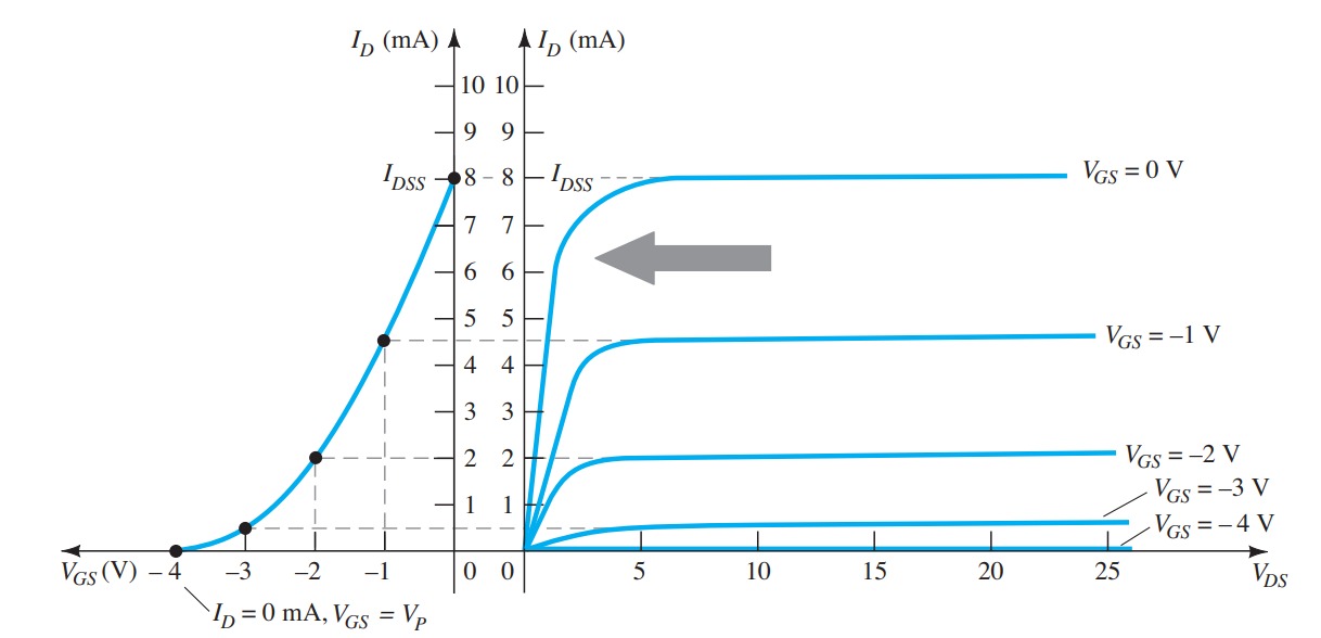
Fig showing the output characteristics of JFET at various VGS
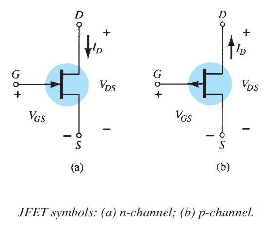
Fig showing the symbol of JFET
Fig showing the output characteristics of p-channel JFET
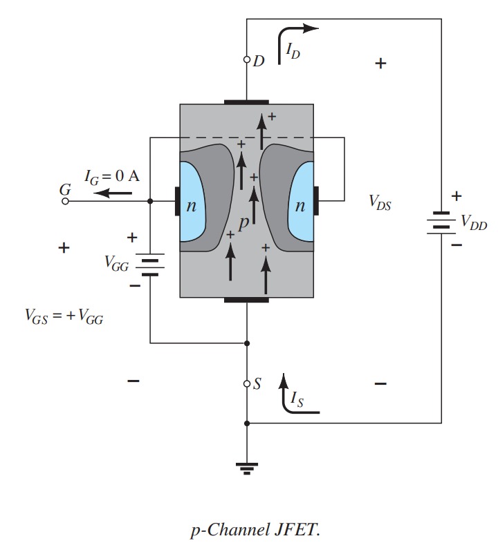
Fig showing the connection diagram of p-channel JFET
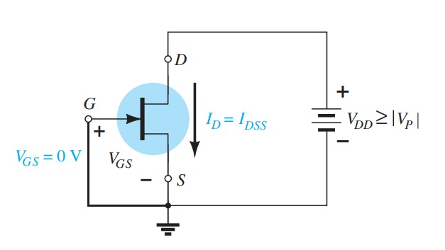
Fig showing the schematic connection of n-channel JFET at VGS=0
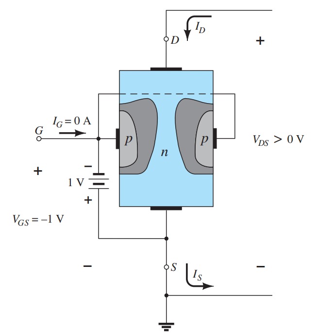
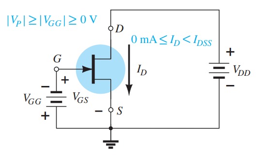
Fig showing the the schematic connection of n-channel JFET at VGS less than 0
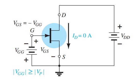
Fig showing the the schematic connection of n-channel JFET at VGS equal to VP
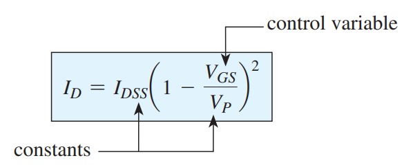
Equation for the Transfer characteristics of JFET
FET Transfer Characteristics
Fig showing the output characteristics and the transfer characteristics
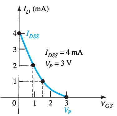
Fig showing the transfer characteristics of p-channel JFET
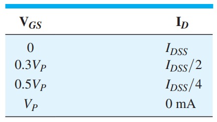
Fig showing the shorthand values of ID at various VGS
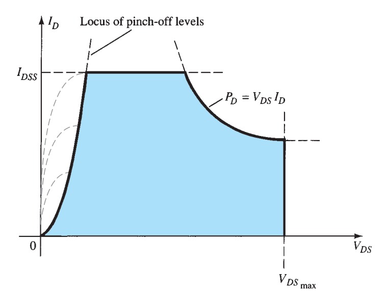
Fig showing the Locus of the Pinch off level and Power limit of JFET
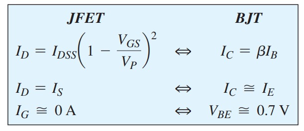
Fig showing the equation relevant to JFET and BJT.
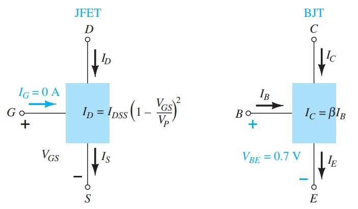
Fig showing the schematic connection and similarity of JFET and BJT.