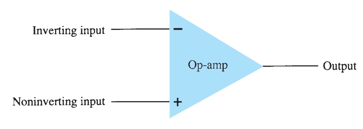
OP-AMPs
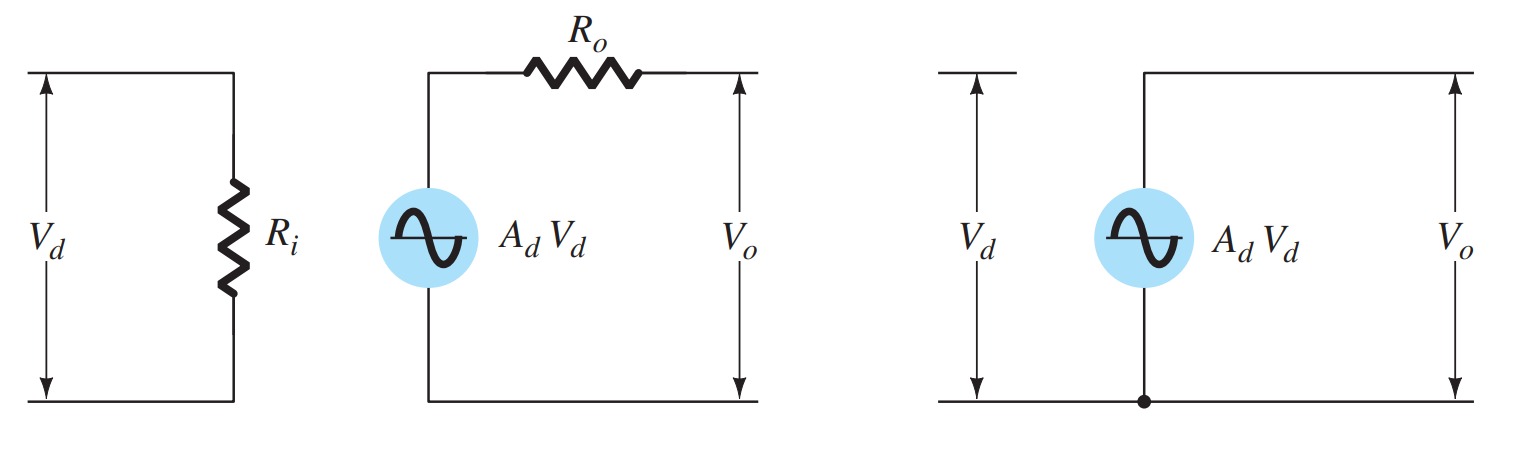
An operational amplifier is a very high gain amplifier having very high input impedance (typically a few megohms) and low output impedance (less than 100 \(\Omega\)). The basic circuit is made using a difference amplifier having two inputs (plus and minus) and at least one output. The plus (+) input produces an output in phase with the signal applied, whereas an input to the minus (-) input results in an opposite-polarity output. The ac equivalent circuit of the op-amp is shown in Fig.
The input signal applied between input terminals sees an input impedance \(R_{i}\) that is typically very high. The output voltage is shown to be the amplifier gain times the input signal taken through an output impedance \(R_{o}\), which is typically very low. An ideal op-amp circuit would have infinite input impedance, zero output impedance, and infinite voltage gain.
Basic Op-Amp
The basic circuit connection is a constant-gain multiplier. An input signal V1 is applied through resistor R1 to the minus input. The output is then connected back to the same minus input through resistor \(R_{f}\). The plus input is connected to ground. Since the signal \(V_{1}\) is essentially applied to the minus input, the resulting output is opposite in phase to the input signal.
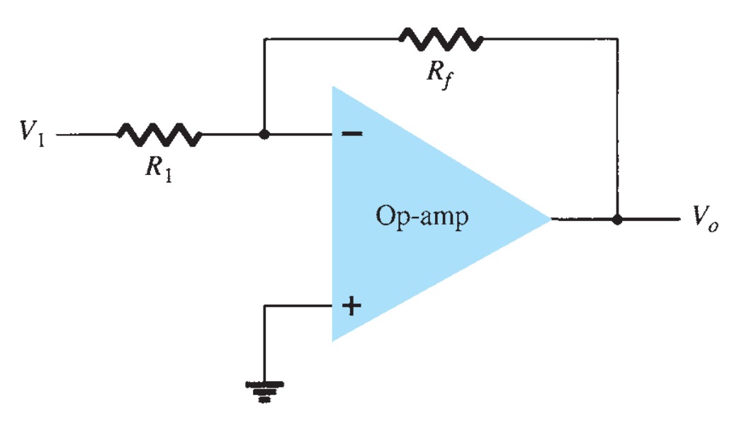
Figure shows the op-amp replaced by its ac equivalent circuit. If we use the ideal op-amp equivalent circuit, replacing \(R_{i}\) by an infinite resistance and \(R_{o}\) by a zero resistance,
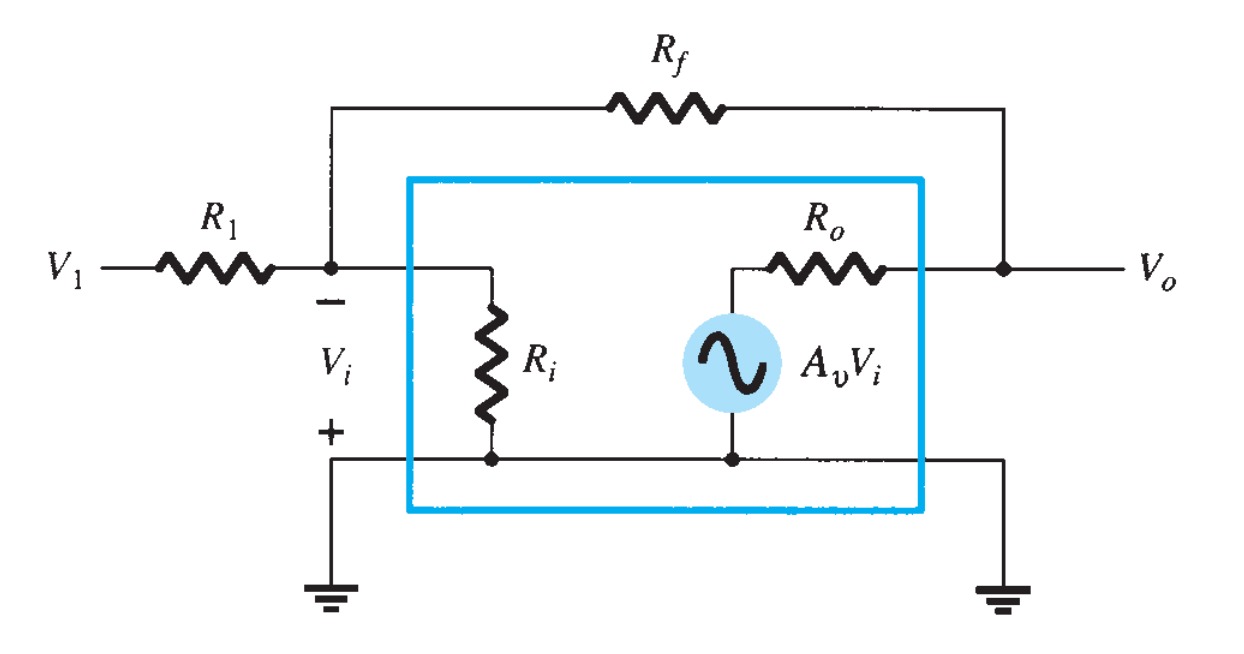
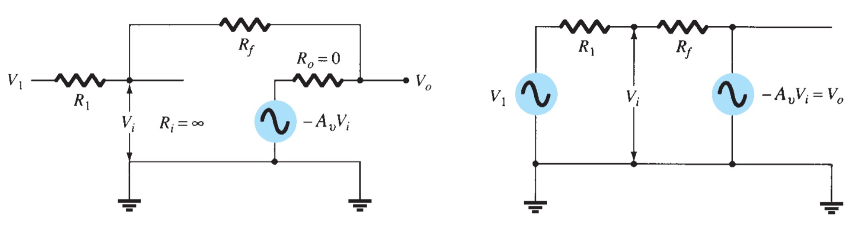
Using superposition, we can solve for the voltage \(V_{1}\) in terms of the components due to each of the sources. For source \(V_{1}\) only (\(-A_{v}V_{i}\) set to zero),
\[V_{i_{1}} = \frac{R_{f}}{R_{1} + R_{f}} V_{1}\]
For source \(-A_{v}V_{i}\) only (\(V_{1}\) set to zero),
\[V_{i_{2}} = \frac{R_{1}}{R_{1} + R_{f}} (-A_{v}V_{i})\]
The total voltage (\(V_{i}\) is then
\[V_{i} = V_{i_{1}} + V_{i_{2}} \]
\[V_{i} = \frac{R_{f}}{R_{1} + R_{f}} V_{1} + \frac{R_{1}}{R_{1} + R_{f}} (-A_{v}V_{i})\]
which can be solved for \(V_{i}\) as
\[V_{i} = \frac{R_{f}}{R_{f} + (1+A_{v})R_{1} } V_{1}\]
If \(A_{v} \gt\gt 1\) and \(A_{v} R_{1} \gt\gt R_{f}\), as is usually true, then
\[V_{i} = \frac{R_{f}}{A_{v}R_{1} } V_{1}\]
Solving for \(V_{o} / V_{i}\), we get
\[\frac{V_{o}}{V_{i}} = \frac{-A_{v}V_{i}}{V_{i}} = \frac{-A_{v}}{V_{i}}\frac{R_{f}V_{1}}{A_{v}R_{1} } = -\frac{R_{f}}{R_{1}}\frac{V_{1}}{V_{i}} \]
so that
\[\frac{V_{o}}{V_{i}} = -\frac{R_{f}}{R_{1}}\]
The result in Eq shows that the ratio of overall output to input voltage is dependent only on the values of resistors \(R_{1}\) and \(R_{ f}\) —provided that \(A_{ v}\) is very large.
Unity Gain
If Rf = R1, the gain is
\[Voltage~gain~(A_{v}) = -\frac{R_{f}}{R_{1}} = -1 \]
so that the circuit provides a unity voltage gain with 180° phase inversion. If \(R_{f}\) is exactly \(R_{1}\), the voltage gain is exactly \(1\).
Constant-Magnitude Gain
If \(R_{f}\) is some multiple of \(R_{1}\), the overall amplifier gain is a constant. For example, if \(R_{f}\) = 10 \(R_{1}\), then
\[Voltage~gain~(A_{v}) = -\frac{R_{f}}{R_{1}} = -10 \]
and the circuit provides a voltage gain of exactly \(10\) along with a 180° phase inversion from the input signal. If we select precise resistor values for \(R_{f}\) and \(R_{1}\), we can obtain a wide range of gains, the gain being as accurate as the resistors used and is only slightly affected by temperature and other circuit factors.
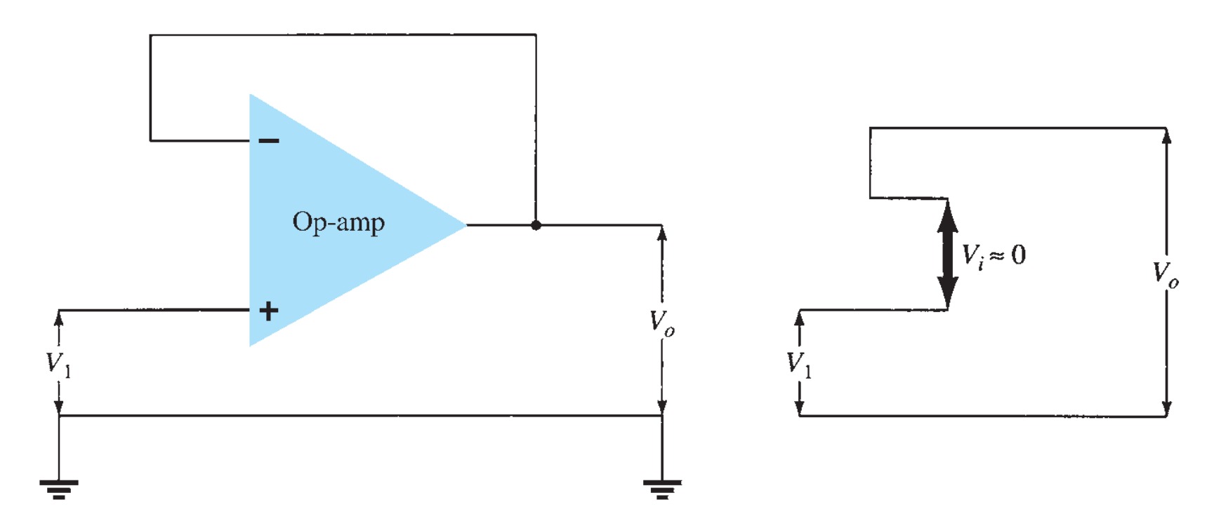
Virtual Ground
The output voltage is limited by the supply voltage of, typically, a few volts. Voltage gains of an Op Amp are very high. If, for example, \(V_{o} = -10\) \(V\) and \(Av = 20,000\), the input voltage is \[V_{i} = \frac{-V_{o}}{A_{v}}= \frac{10}{20,000}~V = 0.5~mV\]
The value of \(V_{i}\) is then small and may be considered \(0\) \(V\). Note that although \(Vi \sim 0\) \(V\), it is not exactly \(0\) \(V\).
The fact that \(Vi \sim 0\) \(V\) leads to the concept that at the amplifier input there exists a virtual short-circuit or virtual ground. The concept of a virtual short implies that although the voltage is nearly \(0\) \(V\), there is no current through the amplifier input to the ground. The figure depicts the virtual ground concept.
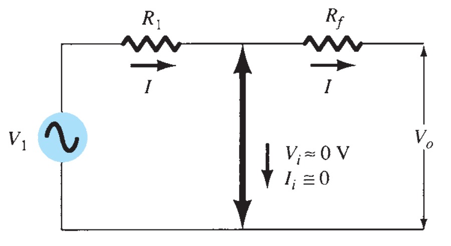
The heavy line is used to indicate that we may consider that a short exists with \(Vi \sim 0\) \(V\) but that this is a virtual short so that no current goes through the short to ground. Current goes only through resistors \(R_{1}\) and \(R_{f}\)
Using the virtual ground concept, we can write equations for the current \(I\) as follows
\[I = \frac{V_{1}}{R_{1}}= -\frac{V_{o}}{R_{f}}\]
which can be solved for \(V_{o}/V_{1}\):
The virtual ground concept, which depends on \(A_{v}\) being very large, allowed a simple solution to determine the overall voltage gain.
Inverting Amplifier
The most widely used constant-gain amplifier circuit is the inverting amplifier.
The output is obtained by multiplying the input by a fixed or constant gain, set by the input resistor (\(R_{1}\)) and feedback resistor (\(R_{f}\))—this output also being inverted from the input.
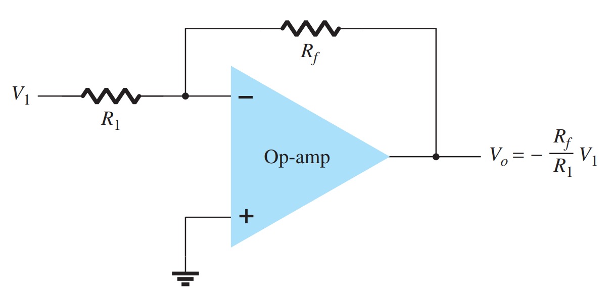
\[V_{o} = -\frac{R_{f}}{R_{1}}\]
Noninverting Amplifier
The connection shows an op-amp circuit that works as a noninverting amplifier or constant-gain multiplier. It should be noted that the inverting amplifier connection is more widely used because it has better frequency stability.
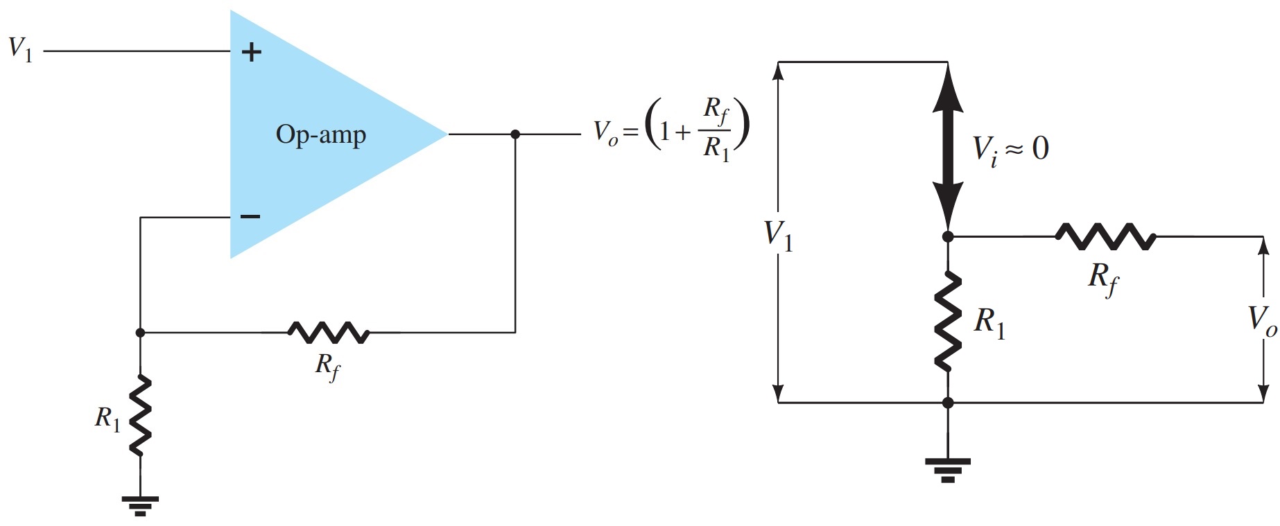
To determine the voltage gain of the circuit, we can use the equivalent representation shown in Fig. Note that the voltage across \(R1\) is \(V1\) since \(Vi \sim 0\) \(V\). This must be equal to the output voltage, through a voltage divider of \(R_{1}\) and \(R_{f}\), so that
\[V_{1} = \frac{R_{1}}{R_{1}+R_{f}}V_{o}\]
which results in
\[\frac{V_{o}}{V_{1}} = \frac{R_{1}+R_{f}}{R_{1}} = 1 + \frac{R_{f}}{R_{1}}\]
Unity Follower
The unity-follower circuit, as shown in Fig, provides a gain of unity (\(1\)) with no polarity or phase reversal. From the equivalent circuit, it is clear that
\[ V_{o} = V_{1} \]
and that the output is the same polarity and magnitude as the input. The circuit operates like an emitter- or source-follower circuit except that the gain is exactly unity.
Summing Amplifier
The most used of the op-amp circuits is the summing amplifier circuit shown in Fig. The circuit shows a three-input summing amplifier circuit, which provides a means of algebraically summing (adding) three voltages, each multiplied by a constant-gain factor. Using the equivalent representation shown in Fig., we can express the output voltage in terms of the inputs as
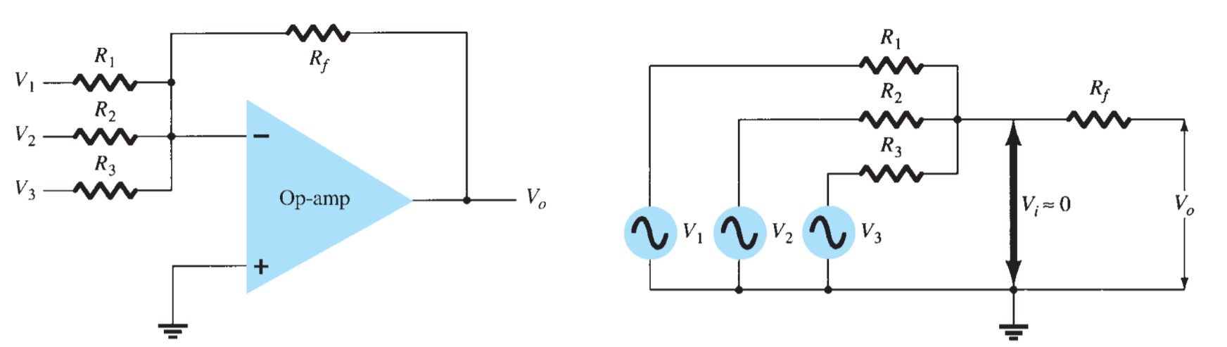
\[V_{o} = -\left(\frac{R_{f}}{R_{1}}V_{o}+\frac{R_{f}}{R_{2}}V_{2}+\frac{R_{f}}{R_{3}}V_{3}\right)\]
In other words, each input adds a voltage to the output multiplied by its separate constant-gain multiplier. If more inputs are used, they each add an additional component to the output.
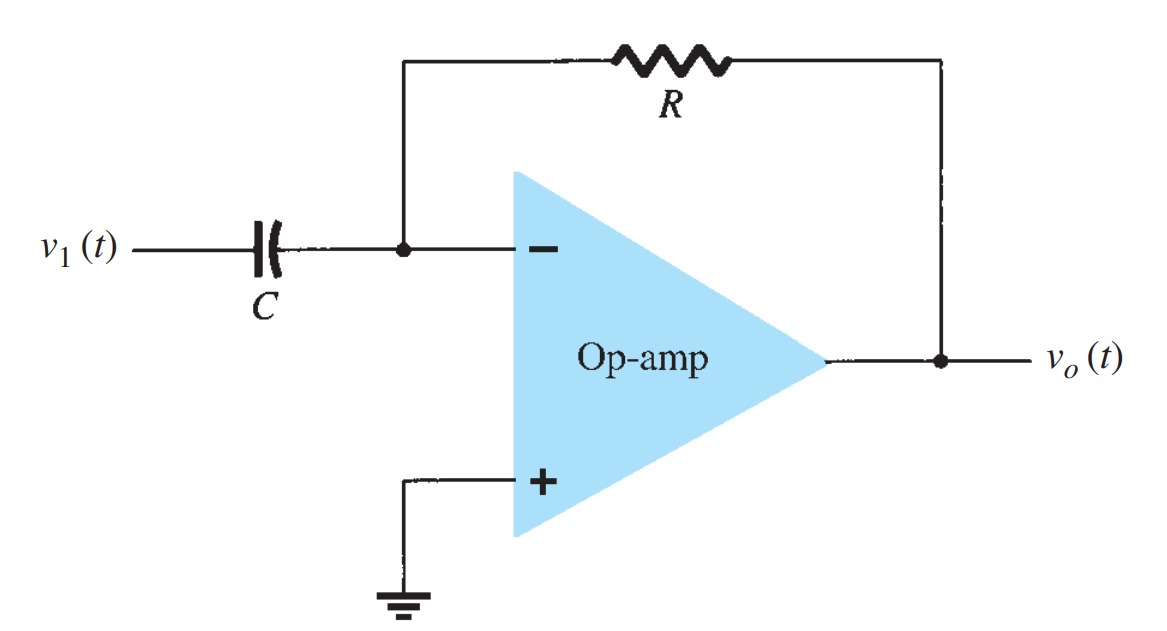
Integrator
The Op Amp integrator is constructed by using a capacitor as the feedback component in instead of resistance in the summing amplifier.
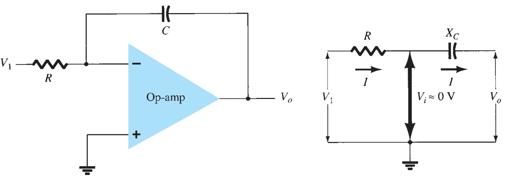
The virtual-ground equivalent circuit shows that an expression for the voltage between input and output can be derived from the current \(I\) from input to output. The virtual ground means that we can consider the voltage at the junction of \(R\) and \(X_{C}\)to be ground (since \(Vi \sim` 0\) \(V\)) but that no current goes into the ground at that point.
The Laplace transform converts integral and differential equations into algebraic equations.
- complex number in Cartesian form: \(z = x + jy\)
- \(x\) = the real part of \(z\)
- \(y\) = the imaginary part of \(z\)
- \(j\) = \(√−1\) (engineering notation); \(i = √−1\) is polite term in mixed company
- complex number in polar form: \(z = re^{j\phi}\)
- \(r\) is the modulus or magnitude of \(z\)
- \(\phi\) is the angle or phase of \(z\)
- \(exp(j\phi) = \cos \phi + j \sin \phi\)
- complex exponential of z = x + jy:
- \(e^{z} = e^{x+jy} = e^{x}e^{jy}\) = \(e^{x}(\cos y + j \sin y\)
The Laplace transform is used in functions defined for \(t \geq 0\) the Laplace transform of a function \(f\) is the function \(F = L(f)\) defined by \[F(s) = \int_{0}^{\infty} f(t)e^{−st}~dt\]
for those \(s\) ∈ C for which the integral makes sense
- \(F\) is a complex-valued function of complex numbers
- \(s\) is called the (complex) frequency variable, with units \(sec^{−1}\); \(t\) is called the time variable (in sec); \(st\) is unitless
- assume \(f\) contains no impulses at \(t = 0\)
common notation convention: lower case letter denotes functions; capital letter denotes its Laplace transform, e.g., \(U\) denotes \(L(u)\), \(V_{in}\) denotes \(L(v_{in})\), etc.
constant: (or unit step) \(f(t)\) = \(1\) (for \(t \geq 0\))
\[F(s) = \int_{0}^{\infty} e^{−st}~dt = −\frac{1}{s}e^{−st}\bigg|_{0}^{\infty} = \frac{1}{s}\]
provided \(e^{−st} → 0\) as \(t → \infty\), which is true for \(RE(z) \gt 0\).
The capacitive impedance can be expressed as
\[X_{C} = \frac{1}{j\omega C} = \frac{1}{sC}\]
where \(s = j\omega\) is in the Laplace notation. Solving for \(V_{o}/V_{1}\) yields
\[I = \frac{V_{1}}{R} = -\frac{V_{o}}{X_{C}} = \frac{-V_{o}}{1/sC} = -sCV_{o}\]
\[\frac{V_{o}}{V_{1}} = \frac{-1}{sCR}\]
This expression can be rewritten in the time domain as
\[v_{o}(t) =-\frac{1}{RC}\int v_{1}(t)~dt\]
The equation shows that the output is the integral of the input, with an inversion and scale multiplier of \(1/RC\). The ability to integrate a given signal provides the analog computer with the ability to solve differential equations and, therefore provides the ability to electrically solve analogs of physical system operation.
The integration operation is one of summation, summing the area under a waveform or a curve over a period of time. If a fixed voltage is applied as input to an integrator circuit, the output voltage grows over a period of time, providing a ramp voltage. The output voltage ramp (for a fixed input voltage) is opposite in polarity to the input voltage and is multiplied by the factor \(1/RC\).
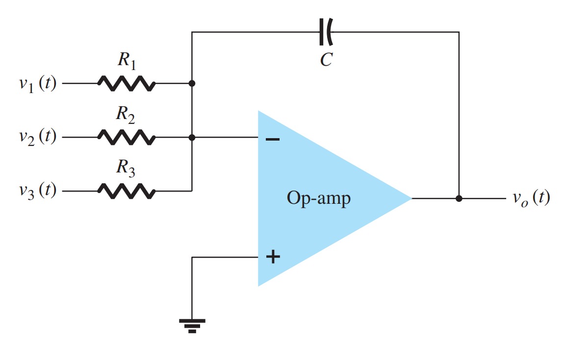
More than one input may be applied to an integrator, as shown in Fig., with the resulting operation given by
\[v_{o}(t) =-\left[\frac{1}{R_{1}C}\int v_{1}(t)~dt+\frac{1}{R_{2}C}\int v_{1}(t)~dt+\frac{1}{R_{3}C}\int v_{1}(t)~dt\right]\]
Differentiator
A differentiator circuit is shown in Fig. Although it is not as useful as the circuit forms covered above, the differentiator does provide a useful operation, the resulting relation for the circuit being
\[vo = -RC \frac{dv_{1}(t)}{dt}\]
where the scale factor is \(-RC\)
Logarithmic and Anti-log Amplifier
The electronic circuits that can perform mathematical operations such as logarithm and anti-logarithm with amplification are called Logarithmic and Anti-Logarithmic amplifiers, respectively. The applications for log/anti-log amplifiers include signal compression and process control.
Log Amplifier
A logarithmic amplifier is an electronic circuit that produces an output proportional to the logarithm of the applied input. An op-amp-based logarithmic amplifier produces a voltage at the output proportional to the logarithm of the voltage applied to the resistor connected to its inverting terminal. The circuit diagram of the op-amp-based logarithmic amplifier is shown in Figure 1.
In the above circuit, the non-inverting input terminal of the op-amp is connected to the ground. That means zero volts are applied at the non-inverting input terminal of the op-amp.
The nodal equation at the inverting input is as follows.
\[0 - \frac{V_{i}}{R_{1}} + I_{f} = 0 ~~~~~~~~~~~~~~~~~~~~~~~~~~~~~~~~~(1)\]
from the equation 1, the feedback current is \[I_{f} = \frac{V_{i}}{R_{1}}\]
When the diode is forward-biased, the current flowing through the diode is \[I_{f} = I_{s}e^{(\frac{V_{f}}{\eta V_{T})}}~~~~~~~~~~~~~~~~~~~~~~~~~~~~~~~~~(2) \] Where, \(I_{s}\) is the saturation current of the diode, \(V_{f}\) is the voltage drop across the diode; when it is in forward bias, \(V_{T}\) is the diode's thermal equivalent voltage. The KVL equation around the feedback loop of the op-amp will be \[0 - V_{f} - V_{0} = 0\]
\[V_{f} = -V_{0}\]
Substituting the value of \(V_{f}\) in Equation 2, we get \[I_{f} = I_{s}e^{-\left(\frac{V_{0}}{\eta V_{T}}\right)} ~~~~~~~~~~~~~~~~~~~~~~~~~~~~~~~~~(3)\]
\[V_{i}/R_{1} = I_{s}e^{-\left(\frac{V_{0}}{\eta V_{T}}\right)}\]
\[V_{i}/R_{1}I_{s} = e^{-\left(\frac{V_{0}}{\eta V_{T}}\right)}\]
Applying natural logarithms on both sides \[\ln\left(\frac{V_{i}}{R_{1}I_{s}}\right) = -\frac{V_{0}}{\eta V_{T}}\]
\[V_{0} = -\eta V_{T}\ln \left(\frac{V_{i}}{R_{1}I_{s}}\right)\]
In the above equation, the parameters \(eta\), \(V_{T}\) and \(I_{s}\) are constants. So, the output voltage \(V_{0}\) will be proportional to the natural logarithm of the input voltage \(V_{i}\) for a fixed value of resistance \(R_{1}\). The output voltage V0 has a negative sign, which indicates that there exists a 180° phase difference between the input and the output.
Antilog Amplifier
An op-amp-based anti-logarithmic amplifier produces a voltage at the output, which is proportional to the anti-logarithm of the voltage that is applied to the diode connected to its inverting input. The circuit diagram of an op-amp-based anti-logarithmic amplifier is shown in Figure 2.
In the circuit shown above, the non-inverting input of the op-amp is connected to the ground. According to the virtual ground concept, the voltage at the inverting input of op-amp will be equal to the voltage present at its non-inverting input. So, the voltage at its inverting input will be zero volts. The nodal equation at the inverting input node is \[-I_{f}+0-V_{0}/R_{f} = 0\]
\[V_{0} = -I_{f} \times R_{f} ~~~~~~~~~~~~~~~~~~~~~~~~~~~~~~~~~(4)\]
When the diode is forward-biased, the current flowing through the diode is given by \[I_{f} = I_{s}e^{\left(\frac{V_{f}}{\eta V_{T}}\right)}\]
Substituting the value of \(I_{f}\) in Equation 4, then \[V_{0} = -R_{f}I_{s}e^{\left(\frac{V_{f}}{\eta V_{T}}\right)}~~~~~~~~~~~~~~~~~~~~~~~~~~~~~~~~~(5)\]
The KVL equation at the inverting input of the op-amp will be \[V_{i} - V_{f} = 0\]
So, \[V_{i} = V_{f}\]
Substituting the value of \(V_{f}\) in equation 5, then \[V_{0} = -R_{f}I_{s}e^{\left(\frac{V_{i}}{\eta V_{T}}\right)}\]
In the above equation, the parameters \(\eta\), \(V_{T}\), and \(I_{s}\) are constants. So, the output voltage \(V_{0}\) will be proportional to the anti-natural logarithm of the input voltage \(V_{i}\) for a fixed value of feedback resistance \(R_{f}\). The output voltage \(V_{0}\) has a negative sign, which indicates that there exists a 180° phase difference between the input and the output.
OP AMP Subtractor
Two signals can be subtracted from one another in a number of ways. Figure shows two op-amp stages used to provide subtraction of input signals. The resulting output is given by
\[V_{o} = - \left[\frac{R_{f}}{R_{3}}\left(\frac{R_{f}}{R_{1}}\right)V_{1} +\frac{R_{f}}{R_{2}}V_{2}\right]\]
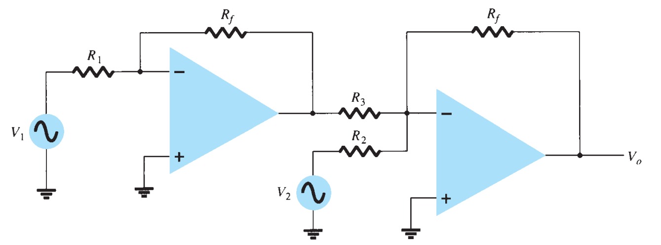
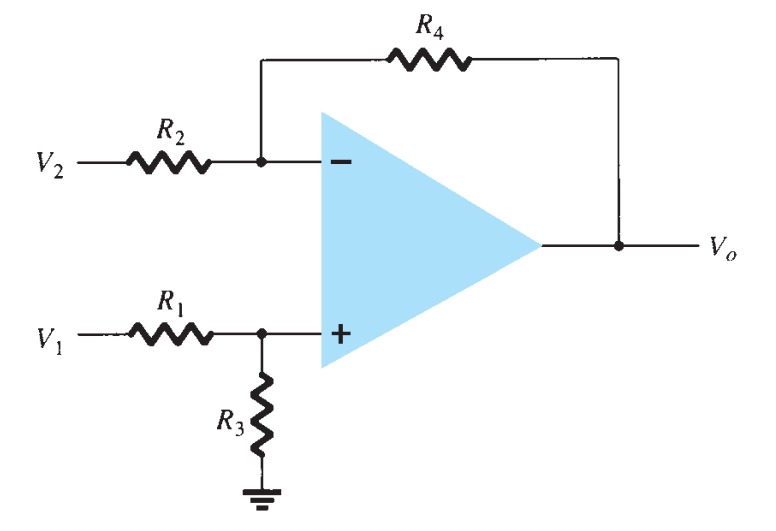
A connection to provide subtraction of two signals is shown in Fig. This connection uses only one op-amp stage to subtract two input signals. Using the superposition principle, the output Vo will be
\[V_{o} = \frac{R_{3}}{R_{1} + R_{3}}\frac{R_{2} + R_{4}}{R_{2}}V_{1} - \frac{R_{4}}{R_{2}}V_{2} \]
Active Filters
A popular application uses op-amps to build active filter circuits. A filter circuit can be constructed using passive components: resistors and capacitors. An active filter additionally uses an amplifier to provide voltage amplification and signal isolation or buffering.
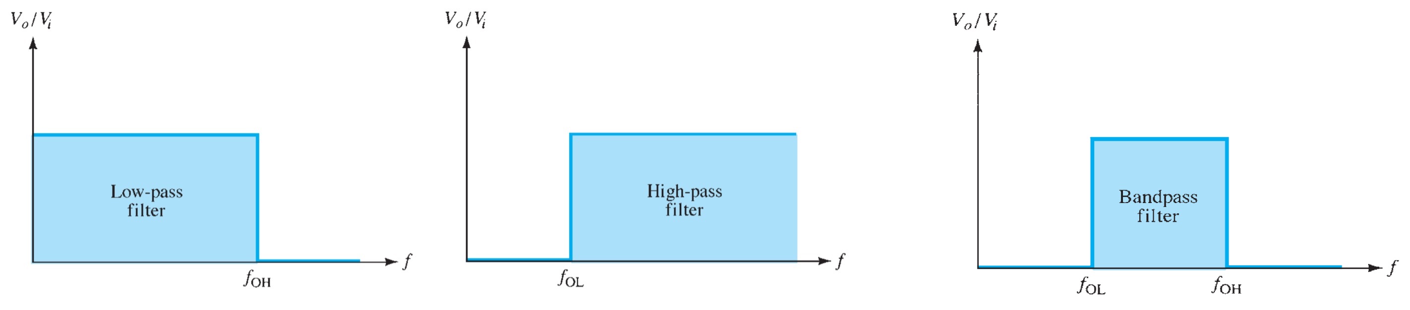
A filter that provides a constant output from dc up to a cutoff frequency \(f_{OH}\) and then passes no signal above that frequency is called an ideal low-pass filter. The ideal response of a low-pass filter is shown in Fig. A filter that provides or passes signals above a cutoff frequency \(f_{OL}\) is a high-pass filter, as idealized in Fig. When the filter circuit passes signals that are above one ideal cutoff frequency and below a second cutoff frequency, it is called a bandpass filter, as idealized in Fig.
Low-Pass Filter
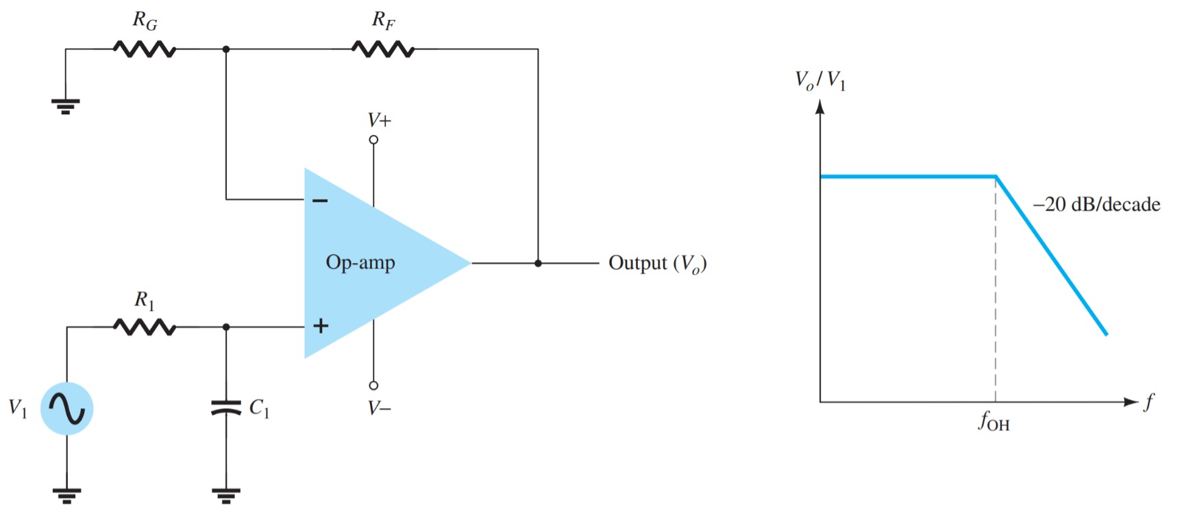
A first-order, low-pass filter using a single resistor and capacitor, as in Fig. has a the practical slope of \(-20\) \(dB\) per decade, as shown in Fig. (rather than the ideal response of Fig. The voltage gain below the cutoff frequency is constant at
\[A_{v} = \left(1 +\frac{R_{F}}{R_{G}}\right) \]
at a cutoff frequency of \[f_{OH} = \frac{1}{2\pi R_{1}C_{1}}\]
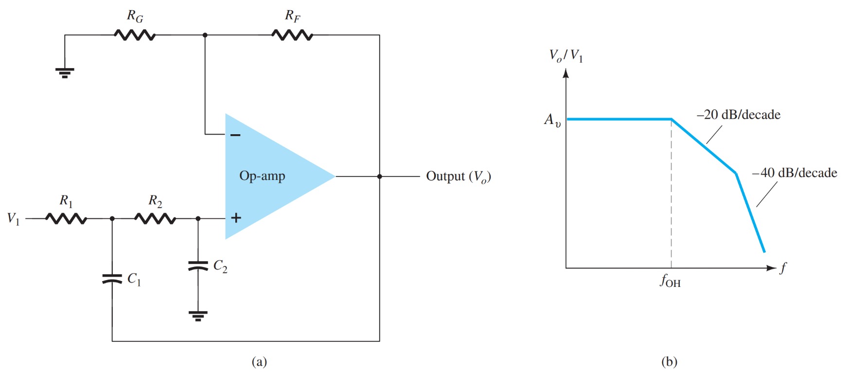
Connecting two sections of the filter as in Fig. results in a second-order low-pass filter with a cutoff at \(-40\) \(dB\) per decade—closer to the ideal characteristic of Fig. The circuit voltage gain and the cutoff frequency are the same for the second-order circuit as for the first-order filter circuit, except that the filter response drops faster for a second-order filter circuit.
High Pass filter
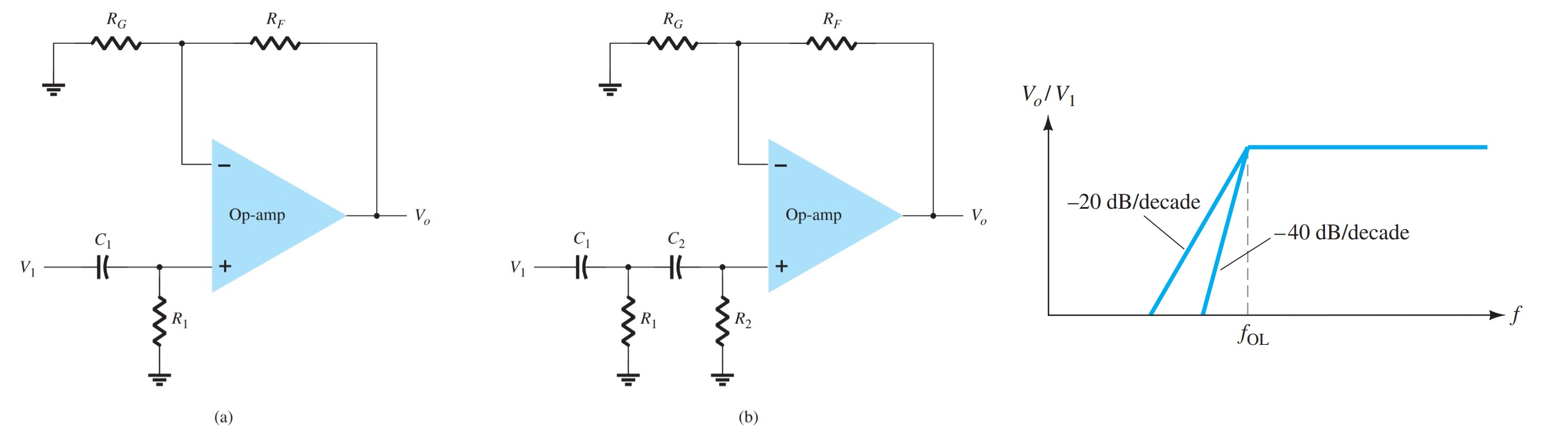
First- and second-order high-pass active filters can be built as shown in Fig. The amplifier gain is calculated using Eq. The amplifier cutoff frequency is
\[f_{OL} = \frac{1}{2\pi R_{1}C_{1}}\]
with a second-order filter \(R_{1} = R_{2}\), and \(C_{1} = C_{2}\) results in the same cutoff frequency as in Eq.
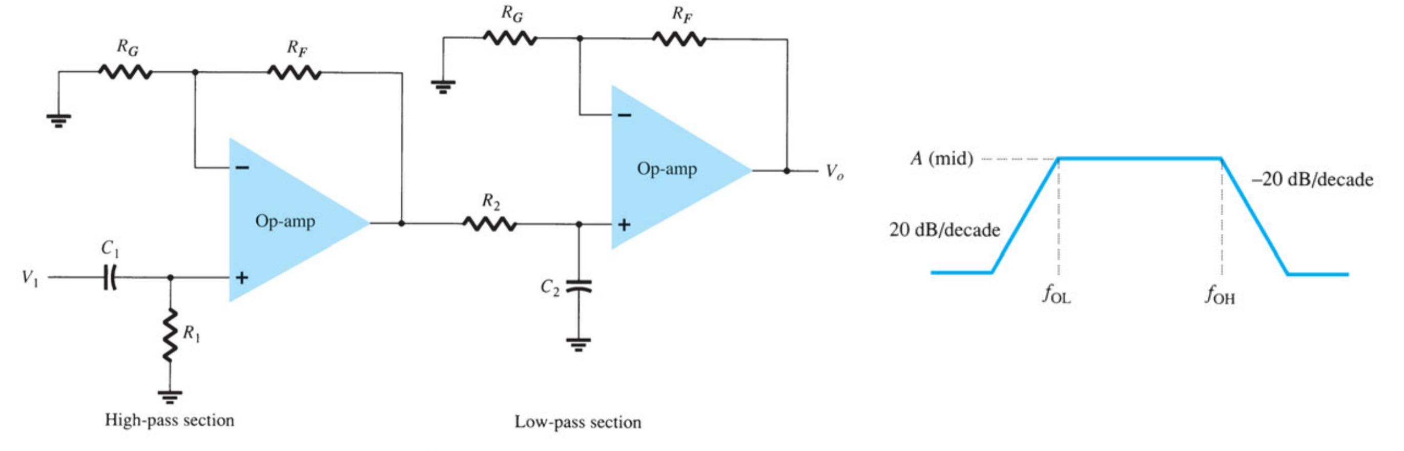
Bandpass Filter
Figure shows a bandpass filter using two stages, the first a high-pass filter and the second a low-pass filter, the combined operation being the desired bandpass response.
OP AMP Specifications
Offset Currents and Voltages
Input Offset Voltage \(V_{IO}\)
The manufacturer's specification sheet provides a value of \(V_{IO}\) for the op-amp
Gain–Bandwidth
An op-amp is designed to be a high-gain, wide-bandwidth amplifier. Op-amp specifications provide a description of the gain versus bandwidth. The frequency band from \(0\) \(Hz\) to the unity-gain frequency (\(f_{1}\)) is its bandwidth. The frequency at which the gain drops by \(3\) \(dB\) (or to \(0.707\) the dc gain, \(A_{VD}\)), this being the cutoff frequency of the op-amp, \(f_{C}\). In fact, the unity-gain frequency and cutoff frequency are related by
\[f_{1} = A_{VD} f_{C}\]
Equation shows that the unity-gain frequency \(f_{1}\) may also be called the gain–bandwidth product of the op-amp.
Slew Rate (\(SR\))
Another parameter reflecting the op-amp’s ability to handle varying signals is the slew rate, defined as
Slew rate = maximum rate at which amplifier output can change in volts per microsecond (\(V/\mu s\))
\[SR = \frac{\Delta V_{o}}{\Delta t}~V/\mu s\]
The slew rate provides a parameter specifying the maximum rate of change of the output voltage when driven by a large step-input signal. If one tried to drive the output at a rate of voltage change greater than the slew rate, the output would not be able to change fast enough and would not vary over the full range expected, resulting in signal clipping or distortion.
Maximum Signal Frequency
The maximum frequency at which an op-amp may operate depends on both the bandwidth (\(BW\)) and slew rate (\(SR\)) parameters of the op-amp. For a sinusoidal signal of general form
\[ v_{o} = K~sin(2\pi ft) \]
the maximum voltage rate of change can be shown to be
\[signal~maximum~rate~of~change = 2\pi fK~V/s \]
To prevent distortion at the output, the rate of change must also be less than the slew rate, that is, \[2\pi f K \leq SR\] \[\omega K \leq SR \] so that \[f \leq \frac{SR}{2pK}~ Hz\] \[ v \leq \frac{SR}{K}~ rad/s\]
Additionally, the maximum frequency \(f\) in Eq. is also limited by the unity-gain bandwidth.
Absolute Maximum Ratings
The absolute maximum ratings provide information on what largest voltage supplies may be used, how large the input signal swing may be, and how much power the device is capable of operating.
Differential and Common Mode operation
Differential Inputs
When separate inputs are applied to the op-amp, the resulting difference signal is the difference between the two inputs.
\[V_{d} = V_{i_{1}} - V_{i_{2}}\]
Common Inputs
When both input signals are the same, a common signal element due to the two inputs can be defined as the average of the sum of the two signals.
\[ V_{c} = \frac{1}{2} (V_{i_{1}} + V_{i_{2}})\]
Output Voltage
Since any signals applied to an op-amp in general have both in-phase and out-of-phase components, the resulting output can be expressed as
\[V_{o} = A_{d}V_{d} + A_{c}V_{c}\]
where
- \(V_{d}\) = difference voltage
- \(V_{c}\) = common voltage
- \(A_{d}\) = differential gain of the amplifier
- \(A_{c}\) = common-mode gain of the amplifier
Common-Mode Rejection Ratio
The common-mode rejection ratio (CMRR), is defined by the following equation:
\[CMRR = \frac{A_{d}}{A_{c}}\]
The value of CMRR can also be expressed in logarithmic terms as
\[CMRR (log) = 20~log_{10}\frac{A_{d}}{A_{c}}~ (dB)\]
Ideally, the value of the CMRR is infinite. Practically, the larger the value of CMRR, the better is the circuit operation.
We can express the output voltage in terms of the value of CMRR as follows:
\[V_{o} = A_{d}V_{d} + A_{c}V_{c} = A_{d}V_{d} \left(1 + \frac{A_{c}V_{c}}{A_{d}V_{d}}\right)\]
Hence,
\[V_{o} = A_{d}V_{d} \left(1 +\frac{1}{CMRR}\frac{V_{c}}{V_{d}}\right)\]
Even when both \(V_{d}\) and \(V_{c}\) components of a signal are present, for large values of CMRR, the output voltage will be due mostly to the difference signal, with the common-mode component greatly reduced or rejected.